- 您現在的位置:買賣IC網 > PDF目錄373970 > AD9882 (Analog Devices, Inc.) Dual Interface for Flat Panel Displays PDF資料下載
參數資料
| 型號: | AD9882 |
| 廠商: | Analog Devices, Inc. |
| 英文描述: | Dual Interface for Flat Panel Displays |
| 中文描述: | 雙接口的平板顯示器 |
| 文件頁數: | 22/36頁 |
| 文件大小: | 370K |
| 代理商: | AD9882 |
第1頁第2頁第3頁第4頁第5頁第6頁第7頁第8頁第9頁第10頁第11頁第12頁第13頁第14頁第15頁第16頁第17頁第18頁第19頁第20頁第21頁當前第22頁第23頁第24頁第25頁第26頁第27頁第28頁第29頁第30頁第31頁第32頁第33頁第34頁第35頁第36頁
REV. A
–22–
AD9882
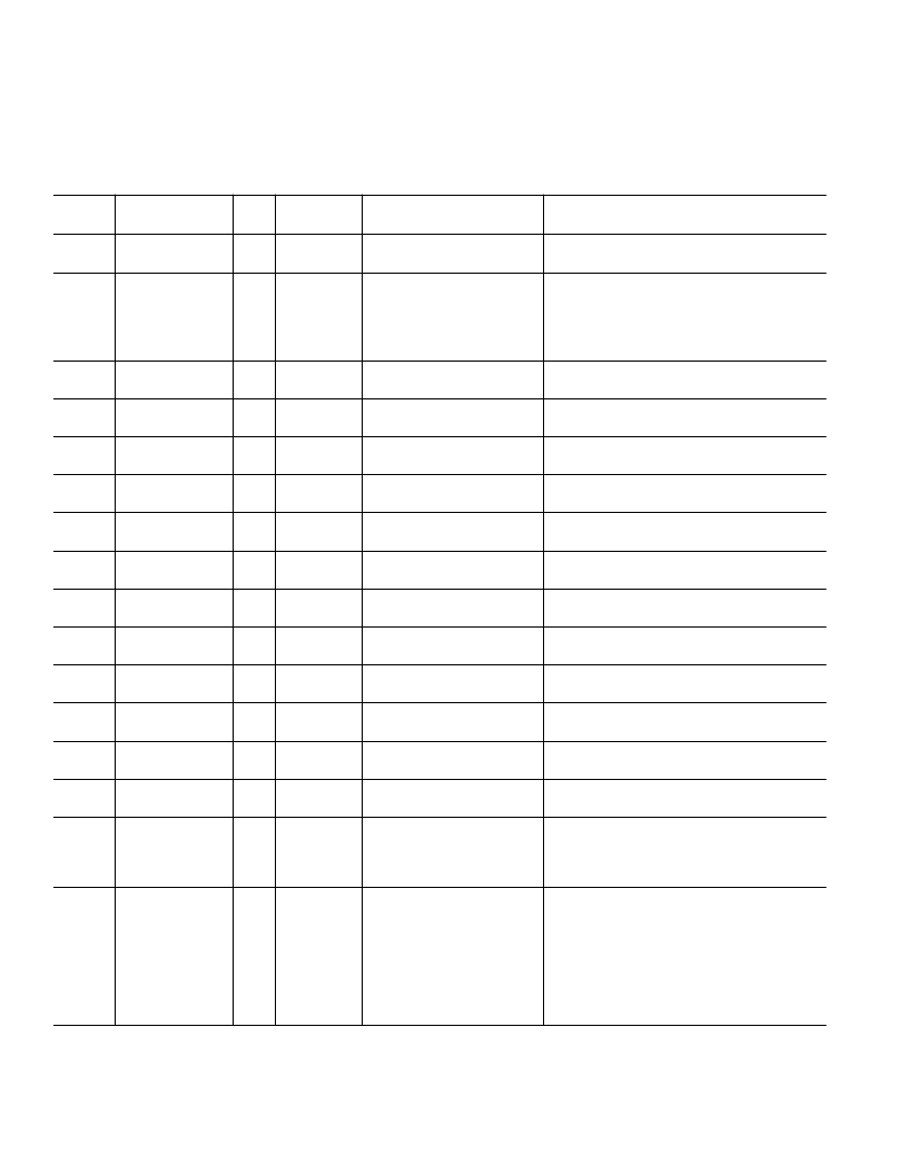
2-WIRE SERIAL REGISTER MAP
The AD9882 is initialized and controlled by a set of registers that determines the operating modes. An external controller is employed
to write and read the Control Registers through the 2-wire serial interface port.
Table IX. Control Register Map
Hex
Address
Read and Write
or Read Only
Default
Value
Bit
Register Name
Function
00
RO
7
–
0
Chip Revisions
An 8-bit register that represents the silicon
level. Revision 0 = 0000 0000
This register is for Bits [11:4] of the PLL
divider. Larger values mean the PLL operates
at a faster rate. This register should be loaded
first whenever a change is needed. (This will
give the PLL more time to lock.)
1
Bits [3:0] LSBs of the PLL divider word. Links
to PLL MSB to make a 12-bit register.
1
Selects VCO frequency range.
Varies the current that drives the PLL loop filter.
ADC clock phase adjustment. Larger values
mean more delay (1 LSB = T/32).
Places the clamp signal an integer number of
clock periods after the trailing edge of Hsync.
Number of clock periods that the clamp signal
is actively clamping.
Sets the number of pixel clocks that HSOUT
will remain active.
Controls the ADC input range (contrast) of the
red channel. Larger values give less contrast.
Controls the ADC input range (contrast) of the
green channel. Larger values give less contrast.
Controls the ADC input range (contrast) of the
blue channel. Larger values give less contrast.
Controls the dc offset (brightness) of the red
channel. Larger values decrease brightness.
Controls the dc offset (brightness) of the green
channel. Larger values decrease brightness.
Controls the dc offset (brightness) of the blue
channel. Larger values decrease brightness.
Sets how many pixel clocks to count before
toggling high or low. This should be set to
some number greater than the maximum
Hsync or equalization pulsewidth.
Sets the voltage level of the Sync-on-Green
slicer
’
s comparator.
0 = No override
1 = User overrides, interface set by 0FH, Bit 1
0 = Analog interface active
1 = Digital interface active
This interface is selected only if Register 0FH,
Bit 2 is set to 1, or if both interfaces are active.
01
R/W
7
–
0
0110 1001
PLL Div MSB
02
R/W
7
–
4
1101
****
PLL Div LSB
03
R/W
7
–
6
5
–
3
7
–
3
01
**
****
**
00 1
***
1000 0
***
VCO Range
Charge Pump
Phase Adjust
04
R/W
05
R/W
7
–
0
0000 1000
Clamp Placement
06
R/W
7
–
0
0001 0100
Clamp Duration
07
R/W
7
–
0
0010 0000
Hsync Output Pulsewidth
08
R/W
7
–
0
1000 0000
Red Gain
09
R/W
7
–
0
1000 0000
Green Gain
0A
R/W
7
–
0
1000 0000
Blue Gain
0B
R/W
7
–
1
1000 000
*
Red Offset
0C
R/W
7
–
1
1000 000
*
Green Offset
0D
R/W
7
–
1
1000 000
*
Blue Offset
0E
R/W
7
–
0
0010 0000
Sync Separator Threshold
0F
R/W
7
–
3
0111 1
***
Sync-On-Green Threshold
2
****
*
0
**
Active Interface Override
1
****
**
0
*
Active Interface Select
NOTE
1
The AD9882 only updates the PLL divide ratio when the LSBs are written to Register 02H.
相關PDF資料 |
PDF描述 |
|---|---|
| AD9883ABST-RL140 | 110 MSPS/140 MSPS Analog Interface for Flat Panel Displays |
| AD9883AKST-110 | 110 MSPS/140 MSPS Analog Interface for Flat Panel Displays |
| AD9883AKST-140 | 110 MSPS/140 MSPS Analog Interface for Flat Panel Displays |
| AD9883A | 110 MSPS/140 MSPS Analog Interface for Flat Panel Displays |
| AD9883ABST-RL110 | 110 MSPS/140 MSPS Analog Interface for Flat Panel Displays |
相關代理商/技術參數 |
參數描述 |
|---|---|
| AD9882/PCB | 制造商:Analog Devices 功能描述:DUAL INTRFC FOR FLAT PNL DISPLAY 100LQFP - Bulk |
| AD9882A | 制造商:AD 制造商全稱:Analog Devices 功能描述:Dual Interface for Flat Panel Displays |
| AD9882A/PCB | 制造商:AD 制造商全稱:Analog Devices 功能描述:Dual Interface for Flat Panel Displays |
| AD9882AKSTZ-100 | 功能描述:IC INTERFACE/DVI 100MHZ 100LQFP RoHS:是 類別:集成電路 (IC) >> 接口 - 專用 系列:- 特色產品:NXP - I2C Interface 標準包裝:1 系列:- 應用:2 通道 I²C 多路復用器 接口:I²C,SM 總線 電源電壓:2.3 V ~ 5.5 V 封裝/外殼:16-TSSOP(0.173",4.40mm 寬) 供應商設備封裝:16-TSSOP 包裝:剪切帶 (CT) 安裝類型:表面貼裝 產品目錄頁面:825 (CN2011-ZH PDF) 其它名稱:568-1854-1 |
| AD9882AKSTZ-140 | 功能描述:IC INTERFACE/DVI 100MHZ 100LQFP RoHS:是 類別:集成電路 (IC) >> 接口 - 專用 系列:- 特色產品:NXP - I2C Interface 標準包裝:1 系列:- 應用:2 通道 I²C 多路復用器 接口:I²C,SM 總線 電源電壓:2.3 V ~ 5.5 V 封裝/外殼:16-TSSOP(0.173",4.40mm 寬) 供應商設備封裝:16-TSSOP 包裝:剪切帶 (CT) 安裝類型:表面貼裝 產品目錄頁面:825 (CN2011-ZH PDF) 其它名稱:568-1854-1 |
發布緊急采購,3分鐘左右您將得到回復。