- 您現在的位置:買賣IC網 > PDF目錄373970 > AD9882 (Analog Devices, Inc.) Dual Interface for Flat Panel Displays PDF資料下載
參數資料
| 型號: | AD9882 |
| 廠商: | Analog Devices, Inc. |
| 英文描述: | Dual Interface for Flat Panel Displays |
| 中文描述: | 雙接口的平板顯示器 |
| 文件頁數: | 19/36頁 |
| 文件大小: | 370K |
| 代理商: | AD9882 |
第1頁第2頁第3頁第4頁第5頁第6頁第7頁第8頁第9頁第10頁第11頁第12頁第13頁第14頁第15頁第16頁第17頁第18頁當前第19頁第20頁第21頁第22頁第23頁第24頁第25頁第26頁第27頁第28頁第29頁第30頁第31頁第32頁第33頁第34頁第35頁第36頁
REV. A
AD9882
–19–
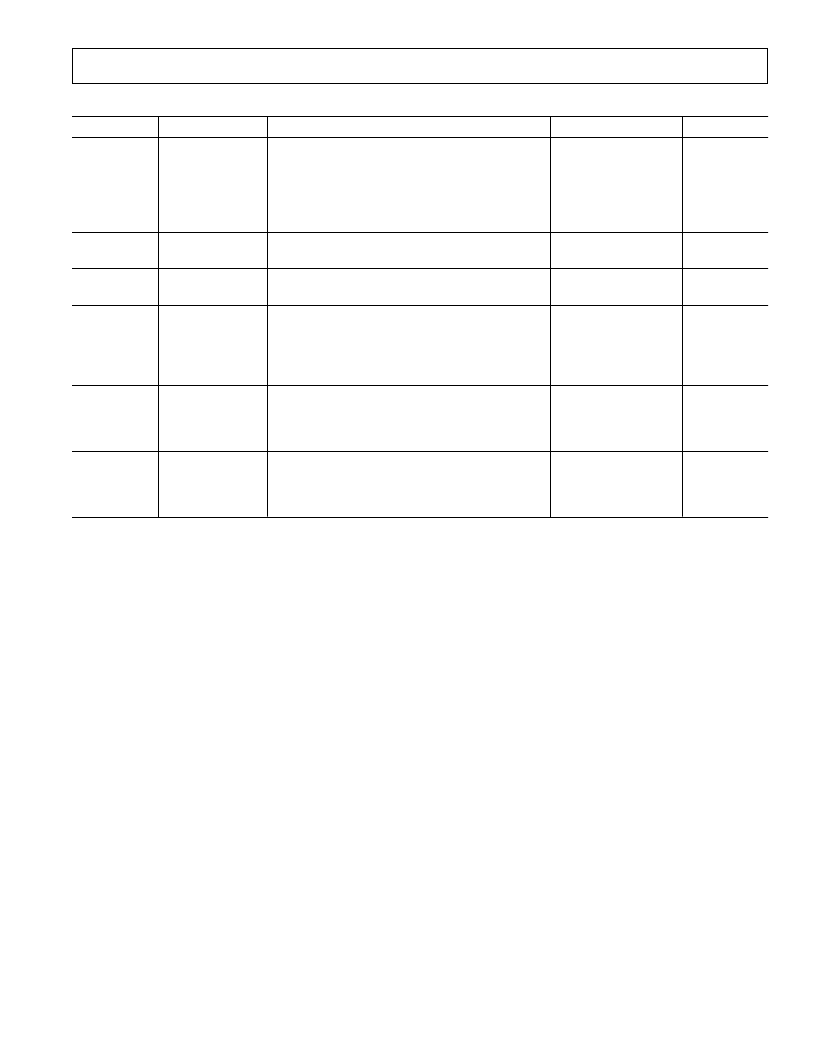
Table VIII. Digital Interface Pin List
Pin Type
Mnemonic
Function
Value
Pin Number
Digital Video
Data Inputs
R
X0+
R
X0
–
R
X1+
R
X1
–
R
X2+
R
X2
–
R
XC+
R
XC
–
R
TERM
Digital Input Channel 0 True
Digital Input Channel 0 Complement
Digital Input Channel 1 True
Digital Input Channel 1 Complement
Digital Input Channel 2 True
Digital Input Channel 2 Complement
33
32
36
35
39
38
Digital Video
Clock Inputs
Digital Data Clock True
Digital Data Clock Complement
41
42
Termination
Control
Control Pin for Setting the Internal Termination
Resistance
28
Outputs
DE
HSOUT
VSOUT
CTL0, CTL1,
CTL2, CTL3
Data Enable
Hsync Output
Vsync Output
Decoded Control Bit Outputs
3.3 V CMOS
3.3 V CMOS
3.3 V CMOS
3.3 V CMOS
86
88
87
22
–
25
HDCP
DDCSCL
DDCSDA
MCL
MDA
HDCP Slave Serial Port Data Clock
HDCP Slave Serial Port Data I/O
HDCP Master Serial Port Data Clock
HDCP Master Serial Port Data I/O
3.3 V CMOS
3.3 V CMOS
3.3 V CMOS
3.3 V CMOS
53
54
81
82
Power Supply
V
D
PV
D
V
DD
GND
Main Power Supply
PLL Power Supply
Output Power Supply
Ground Supply
3.15 V to 3.45 V
3.15 V to 3.45 V
2.2 V to 3.6 V
0 V
DIGITAL INTERFACE PIN DESCRIPTIONS
DIGITAL DATA INPUTS
R
X0+
Positive Differential Input Data (Channel 0)
R
X0
–
Negative Differential Input Data (Channel 0)
R
X1+
Positive Differential Input Data (Channel 1)
R
X1
–
Negative Differential Input Data (Channel 1)
R
X2+
Positive Differential Input Data (Channel 2)
R
X2
–
Negative Differential Input Data (Channel 2)
These six pins receive three pairs of differential, low voltage swing input pixel
data from a DVI transmitter.
DIGITAL CLOCK INPUTS
R
XC+
R
XC
–
These two pins receive the differential, low voltage swing input pixel clock from
a DVI transmitter.
Positive Differential Input Clock
Negative Differential Input Clock
TERMINATION CONTROL
R
TERM
Internal Termination Set Pin
This pin is used to set the termination resistance
for all of the digital interface high speed inputs.
To set, place a resistor of value equal to 10
¥
the
desired input termination resistance between this
pin (Pin 28) and ground supply. Typically, the
value of this resistor should be 500
W
.
OUTPUTS
DE
Data Enable Output
This pin outputs the state of data enable (DE).
The AD9882 decodes DE from the incoming
stream of data. The DE signal will be HIGH
during active video and will be LOW while there
is no active video.
HDCP Slave Serial Port Data Clock
For use in communicating with the HDCP
enabled DVI transmitter.
HDCP Slave Serial Port I/O
For use in communicating with the HDCP
enabled DVI transmitter.
HDCP Master Serial Port Data Clock
Connects to the EEPROM for reading the
encrypted HDCP keys.
HDCP Master Serial Port Data I/O
Connects to the EEPROM for reading the
encrypted HDCP keys.
Digital Control Outputs
These pins output the control signals for the
Red and Green channels. CTL0 and CTL1
correspond to the Red channel
’
s input, while
CTL2 and CTL3 correspond to the Green
channel
’
s input.
DDCSCL
DDCSDA
MCL
MDA
CTL
相關PDF資料 |
PDF描述 |
|---|---|
| AD9883ABST-RL140 | 110 MSPS/140 MSPS Analog Interface for Flat Panel Displays |
| AD9883AKST-110 | 110 MSPS/140 MSPS Analog Interface for Flat Panel Displays |
| AD9883AKST-140 | 110 MSPS/140 MSPS Analog Interface for Flat Panel Displays |
| AD9883A | 110 MSPS/140 MSPS Analog Interface for Flat Panel Displays |
| AD9883ABST-RL110 | 110 MSPS/140 MSPS Analog Interface for Flat Panel Displays |
相關代理商/技術參數 |
參數描述 |
|---|---|
| AD9882/PCB | 制造商:Analog Devices 功能描述:DUAL INTRFC FOR FLAT PNL DISPLAY 100LQFP - Bulk |
| AD9882A | 制造商:AD 制造商全稱:Analog Devices 功能描述:Dual Interface for Flat Panel Displays |
| AD9882A/PCB | 制造商:AD 制造商全稱:Analog Devices 功能描述:Dual Interface for Flat Panel Displays |
| AD9882AKSTZ-100 | 功能描述:IC INTERFACE/DVI 100MHZ 100LQFP RoHS:是 類別:集成電路 (IC) >> 接口 - 專用 系列:- 特色產品:NXP - I2C Interface 標準包裝:1 系列:- 應用:2 通道 I²C 多路復用器 接口:I²C,SM 總線 電源電壓:2.3 V ~ 5.5 V 封裝/外殼:16-TSSOP(0.173",4.40mm 寬) 供應商設備封裝:16-TSSOP 包裝:剪切帶 (CT) 安裝類型:表面貼裝 產品目錄頁面:825 (CN2011-ZH PDF) 其它名稱:568-1854-1 |
| AD9882AKSTZ-140 | 功能描述:IC INTERFACE/DVI 100MHZ 100LQFP RoHS:是 類別:集成電路 (IC) >> 接口 - 專用 系列:- 特色產品:NXP - I2C Interface 標準包裝:1 系列:- 應用:2 通道 I²C 多路復用器 接口:I²C,SM 總線 電源電壓:2.3 V ~ 5.5 V 封裝/外殼:16-TSSOP(0.173",4.40mm 寬) 供應商設備封裝:16-TSSOP 包裝:剪切帶 (CT) 安裝類型:表面貼裝 產品目錄頁面:825 (CN2011-ZH PDF) 其它名稱:568-1854-1 |
發布緊急采購,3分鐘左右您將得到回復。