- 您現在的位置:買賣IC網 > PDF目錄373924 > AD7893 (Analog Devices, Inc.) 14-Bit 50 kSPS ADC Ser. Out, 1.8V Operation 8-MSOP PDF資料下載
參數資料
| 型號: | AD7893 |
| 廠商: | Analog Devices, Inc. |
| 英文描述: | 14-Bit 50 kSPS ADC Ser. Out, 1.8V Operation 8-MSOP |
| 中文描述: | LC2MOS 12位,串行ADC的6我們在8引腳封裝 |
| 文件頁數: | 3/12頁 |
| 文件大小: | 340K |
| 代理商: | AD7893 |
AD7893
–3–
REV. E
TIMING CHARACTERISTICS
1, 2
A, B
Versions
S
Version
Parameter
Units
Test Conditions/Comments
t
1
t
2
t
3
t
43
t
54
50
60
30
50
10
100
50
70
40
60
10
100
ns min
ns min
ns min
ns max
ns min
ns max
CONVST
Pulse Width
SCLK High Pulse Width
SCLK Low Pulse Width
SCLK Rising Edge to Data Valid Delay
Bus Relinquish Time after Falling Edge of SCLK
NOTES
1
Sample tested at +25
°
C to ensure compliance. All input signals are measured with tr = tf = 1 ns (10% to 90% of +5 V) and timed from a voltage level of +1.6 V.
2
See Figure 5.
3
Measured with the load circuit of Figure 1 and defined as the time required for an output to cross 0.8 V or 2.4 V.
4
Derived from the measured time taken by the data outputs to change 0.5 V when loaded with the circuit of Figure 1. The measured number is then extrapolated back
to remove the effects of charging or discharging the 50 pF capacitor. This means that the time, t
5
, quoted in the timing characteristics is the true bus relinquish time
of the part and, as such, is independent of external bus loading capacitances.
(V
DD
= +5 V, AGND = DGND = 0 V, REF IN = +2.5 V)
ABSOLUTE MAXIMUM RATINGS*
(T
A
= +25
°
C unless otherwise noted)
V
DD
to AGND . . . . . . . . . . . . . . . . . . . . . . . . . –0.3 V to +7 V
V
DD
to DGND . . . . . . . . . . . . . . . . . . . . . . . . . –0.3 V to +7 V
Analog Input Voltage to AGND
AD7893-10, AD7893-5 . . . . . . . . . . . . . . . . . . . . . . .
±
17 V
AD7893-2, AD7893-3 . . . . . . . . . . . . . . . . . . . –5 V, +10 V
Reference Input Voltage to AGND . . . –0.3 V to V
DD
+ 0.3 V
Digital Input Voltage to DGND . . . . . –0.3 V to V
DD
+ 0.3 V
Digital Output Voltage to DGND . . . . –0.3 V to V
DD
+ 0.3 V
Operating Temperature Range
Commercial (A, B Versions) . . . . . . . . . . . –40
°
C to +85
°
C
Extended (S Version) . . . . . . . . . . . . . . . . –55
°
C to +125
°
C
Storage Temperature Range . . . . . . . . . . . . –65
°
C to +150
°
C
Junction Temperature . . . . . . . . . . . . . . . . . . . . . . . . . +150
°
C
Plastic DIP Package, Power Dissipation . . . . . . . . . . 450 mW
θ
JA
Thermal Impedance . . . . . . . . . . . . . . . . . . . . . 130
°
C/W
Lead Temperature (Soldering, 10 sec) . . . . . . . . . . . +260
°
C
Cerdip Package, Power Dissipation . . . . . . . . . . . . . . 450 mW
θ
JA
Thermal Impedance . . . . . . . . . . . . . . . . . . . . . 125
°
C/W
Lead Temperature (Soldering, 10 sec) . . . . . . . . . . . +300
°
C
SOIC Package, Power Dissipation . . . . . . . . . . . . . . . 450 mW
θ
JA
Thermal Impedance . . . . . . . . . . . . . . . . . . . . . 170
°
C/W
Lead Temperature, Soldering
Vapor Phase (60 sec) . . . . . . . . . . . . . . . . . . . . . . +215
°
C
Infrared (15 sec) . . . . . . . . . . . . . . . . . . . . . . . . . . +220
°
C
*Stresses above those listed under “Absolute Maximum Ratings” may cause
permanent damage to the device. This is a stress rating only; functional operation
of the device at these or any other conditions above those listed in the operational
sections of this specification is not implied. Exposure to absolute maximum rating
conditions for extended periods may affect device reliability.
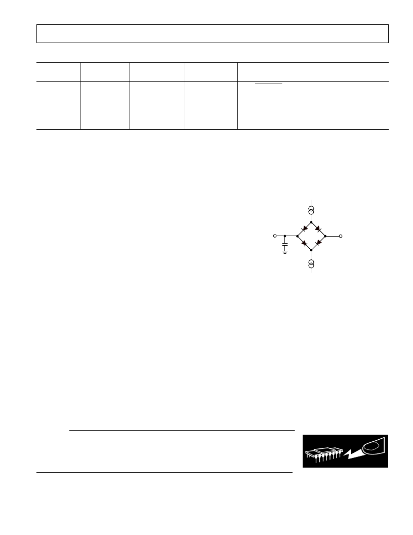
TO
OUTPUT
PIN
+2.1V
1.6mA
200μA
50pF
Figure 1. Load Circuit for Access Time and Bus
Relinquish Time
WARNING!
ESD SENSITIVE DEVICE
CAUTION
ESD (electrostatic discharge) sensitive device. Electrostatic charges as high as 4000 V readily
accumulate on the human body and test equipment and can discharge without detection. Although
the AD7893 features proprietary ESD protection circuitry, permanent damage may occur on devices
subjected to high energy electrostatic discharges. Therefore, proper ESD precautions are
recommended to avoid performance degradation or loss of functionality.
相關PDF資料 |
PDF描述 |
|---|---|
| AD7893AR | Ultralow Power Single/Dual Comparator with Reference; Package: PDIP; No of Pins: 8; Temperature Range: -40°C to +85°C |
| AD7893BN | Ultralow Power Quad Comparators with Reference; Package: PDIP; No of Pins: 16; Temperature Range: 0°C to +70°C |
| AD7893BR | Ultralow Power Quad Comparators with Reference; Package: PDIP; No of Pins: 16; Temperature Range: -40°C to +85°C |
| AD7893SQ | Ultralow Power Quad Comparators with Reference; Package: SO; No of Pins: 16; Temperature Range: -40°C to +85°C |
| AD7893AR-2 | RECTIFIER SCHOTTKY DUAL COMMON-CATHODE 30A 30V 260A-Ifsm 0.57Vf 1A-IR TO-220AB 50/TUBE |
相關代理商/技術參數 |
參數描述 |
|---|---|
| AD7893ACHIPS-10 | 功能描述:12 Bit Analog to Digital Converter 1 Input 1 SAR Die 制造商:analog devices inc. 系列:- 包裝:托盤 - 晶粒 零件狀態:上次購買時間 位數:12 采樣率(每秒):117k 輸入數:1 輸入類型:單端 數據接口:SPI 配置:S/H-ADC 無線電 - S/H:ADC:1:1 A/D 轉換器數:1 架構:SAR 參考類型:外部 電壓 - 電源,模擬:5V 電壓 - 電源,數字:5V 特性:- 工作溫度:-40°C ~ 85°C 封裝/外殼:模具 供應商器件封裝:模具 標準包裝:1 |
| AD7893ACHIPS-2 | 功能描述:12 Bit Analog to Digital Converter 1 Input 1 SAR Die 制造商:analog devices inc. 系列:- 包裝:管件 零件狀態:上次購買時間 位數:12 采樣率(每秒):117k 輸入數:1 輸入類型:單端 數據接口:SPI 配置:S/H-ADC 無線電 - S/H:ADC:1:1 A/D 轉換器數:1 架構:SAR 參考類型:外部 電壓 - 電源,模擬:5V 電壓 - 電源,數字:5V 特性:- 工作溫度:-40°C ~ 85°C 封裝/外殼:模具 供應商器件封裝:模具 標準包裝:1 |
| AD7893ACHIPS-5 | 功能描述:12 Bit Analog to Digital Converter 1 Input 1 SAR Die 制造商:analog devices inc. 系列:- 包裝:托盤 - 晶粒 零件狀態:上次購買時間 位數:12 采樣率(每秒):117k 輸入數:1 輸入類型:單端 數據接口:SPI 配置:S/H-ADC 無線電 - S/H:ADC:1:1 A/D 轉換器數:1 架構:SAR 參考類型:外部 電壓 - 電源,模擬:5V 電壓 - 電源,數字:5V 特性:- 工作溫度:-40°C ~ 85°C 封裝/外殼:模具 供應商器件封裝:模具 標準包裝:1 |
| AD7893AN-10 | 功能描述:IC ADC 12BIT SRL T/H LP 8-DIP RoHS:否 類別:集成電路 (IC) >> 數據采集 - 模數轉換器 系列:- 標準包裝:1 系列:- 位數:14 采樣率(每秒):83k 數據接口:串行,并聯 轉換器數目:1 功率耗散(最大):95mW 電壓電源:雙 ± 工作溫度:0°C ~ 70°C 安裝類型:通孔 封裝/外殼:28-DIP(0.600",15.24mm) 供應商設備封裝:28-PDIP 包裝:管件 輸入數目和類型:1 個單端,雙極 |
| AD7893AN-10Z | 制造商:Analog Devices 功能描述:ADC 12BIT LC2MOS 1LSB 8DIP 制造商:Analog Devices 功能描述:ADC, 12BIT, LC2MOS, 1LSB, 8DIP; Resolution (Bits):12bit; Sampling Rate:117kSPS; Supply Voltage Type:Single; Supply Voltage Min:4.75V; Supply Voltage Max:5.25V; Supply Current:9mA; Digital IC Case Style:DIP; No. of Pins:8; Input ;RoHS Compliant: Yes |
發布緊急采購,3分鐘左右您將得到回復。