- 您現(xiàn)在的位置:買賣IC網(wǎng) > PDF目錄373924 > AD7893 (Analog Devices, Inc.) 14-Bit 50 kSPS ADC Ser. Out, 1.8V Operation 8-MSOP PDF資料下載
參數(shù)資料
| 型號: | AD7893 |
| 廠商: | Analog Devices, Inc. |
| 英文描述: | 14-Bit 50 kSPS ADC Ser. Out, 1.8V Operation 8-MSOP |
| 中文描述: | LC2MOS 12位,串行ADC的6我們在8引腳封裝 |
| 文件頁數(shù): | 10/12頁 |
| 文件大小: | 340K |
| 代理商: | AD7893 |
AD7893
REV. E
–10–
AD7893–ADSP-2105 Interface
An interface circuit between the AD7893 and the ADSP-2105
DSP processor is shown in Figure 8. In the interface shown, the
RFS1 output from the ADSP-2105’s SPORT1 serial port is
used to gate the serial clock (SCLK1) of the ADSP-2105 before
it is applied to the SCLK input of the AD7893. The RFS1 out-
put is configured for active high operation. The interface
ensures a noncontinuous clock for the AD7893’s serial clock
input with only sixteen serial clock pulses provided, and the
serial clock line of the AD7893 remaining low between data
transfers. The SDATA line from the AD7893 is connected to
the DR1 line of the ADSP-2105’s serial port.
AD7893
SDATA
SCLK
ADSP-2105
DR1
RFS1
SCLK1
Figure 8. AD7893 to ADSP-2105 Interface
The timing relationship between the SCLK1 and RFS1 outputs
of the ADSP-2105 are such that the delay between the rising
edge of the SCLK1 and the rising edge of an active high RFS1
is up to 25 ns. There is also a requirement that data must be set
up 10 ns prior to the falling edge of the SCLK1 to be read cor-
rectly by the ADSP-2105. The data access time for the AD7893
is 50 ns from the rising edge of its SCLK input. Assuming a
10 ns propagation delay through the external AND gate, the
high time of the SCLK1 output of the ADSP-2105 must be
≥
(50 + 25 + 10 + 10) ns, i.e.,
≥
95 ns. This means that the
serial clock frequency with which the interface of Figure 13 can
work with is limited to 5.26 MHz.
An alternative scheme is to configure the ADSP-2105 to accept
an external serial clock. In this case, an external noncontinuous
serial clock that drives the serial clock inputs of both the ADSP-
2105 and the AD7893 is provided. In this scheme, the serial
clock frequency is limited to 5 MHz by the ADSP-2105.
To monitor the conversion time on the AD7893, a scheme such
as outlined in previous interfaces with
CONVST
can be used.
This can be implemented by connecting the
CONVST
line
directly to the
IRQ2
input of the ADSP-2105.
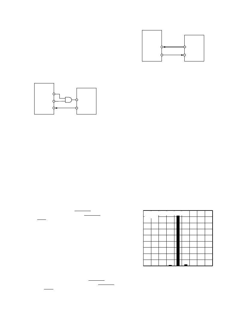
AD7893–DSP56000 Interface
Figure 9 shows an interface circuit between the AD7893 and the
DSP56000 DSP processor. The DSP5600 is configured for nor-
mal mode asynchronous operation with gated clock. It is also set
up for a 16-bit word with the gated serial clock being generated
by the DSP56000 and appears on the SC0 pin. The SC0 pin
should be configured as an output by setting bit SCD0 to 1. In
this mode, the DSP56000 provides sixteen serial clock pulses to
the AD7893 in a serial read operation. The DSP56000 assumes
valid data on the first falling edge of SCK, so the interface is
simply two-wire as shown in Figure 9.
To monitor the conversion time on the AD7893, a scheme such
as outlined in previous interface examples with
CONVST
can
be used. This can be implemented by connecting the
CONVST
line directly to the
IRQA
input of the DSP56000.
AD7893
SDATA
SCLK
DSP56000
SC0
SRD
Figure 9. AD7893 to DSP56000 Interface
AD7893 PERFORMANCE
Linearity
The linearity of the AD7893 is determined by the on-chip 12-bit
D/A converter. This is a segmented DAC that is laser trimmed
for 12-bit integral linearity and differential linearity. Typical
relative numbers for the part are
±
1/4 LSB, while the typical
DNL errors are
±
1/2 LSB.
Noise
In an A/D converter, noise exhibits itself as code uncertainty in
dc applications and as the noise floor (in an FFT, for example)
in ac applications. In a sampling A/D converter like the AD7893,
all information about the analog input appears in the baseband
from dc to 1/2 the sampling frequency. The input bandwidth of
the track/hold exceeds the Nyquist bandwidth; therefore, an
antialiasing filter should be used to remove unwanted signals
above f
S
/2 in the input signal in applications where such signals
exist.
Figure 10 shows a histogram plot for 8192 conversions of a dc
input using the AD7893. The analog input was set at the center
of a code transition. The timing and control sequence used was
per Figure 3 where the optimum performance of the ADC was
achieved. It can be seen that almost all the codes appear in the
one output bin, indicating very good noise performance from
the ADC. The rms noise performance for the AD7893-2 for the
above plot was 87
μ
V. Since the analog input range, and hence
LSB size, on the AD7893-10 is eight times what it is for the
AD7893-2, the same output code distribution results in an out-
put rms noise of 700
μ
V for the AD7893-10.
CODE
9000
1000
(X–4) (X–3)
O
(X–2) (X–1)
X
(X+1) (X+2) (X+3) (X+4)
8000
5000
4000
3000
2000
7000
6000
0
SAMPLING FREQUENCY = 102.4kHz
T
A
= +25
°
C
Figure 10. Histogram of 8192 Conversions of a DC Input
相關(guān)PDF資料 |
PDF描述 |
|---|---|
| AD7893AR | Ultralow Power Single/Dual Comparator with Reference; Package: PDIP; No of Pins: 8; Temperature Range: -40°C to +85°C |
| AD7893BN | Ultralow Power Quad Comparators with Reference; Package: PDIP; No of Pins: 16; Temperature Range: 0°C to +70°C |
| AD7893BR | Ultralow Power Quad Comparators with Reference; Package: PDIP; No of Pins: 16; Temperature Range: -40°C to +85°C |
| AD7893SQ | Ultralow Power Quad Comparators with Reference; Package: SO; No of Pins: 16; Temperature Range: -40°C to +85°C |
| AD7893AR-2 | RECTIFIER SCHOTTKY DUAL COMMON-CATHODE 30A 30V 260A-Ifsm 0.57Vf 1A-IR TO-220AB 50/TUBE |
相關(guān)代理商/技術(shù)參數(shù) |
參數(shù)描述 |
|---|---|
| AD7893ACHIPS-10 | 功能描述:12 Bit Analog to Digital Converter 1 Input 1 SAR Die 制造商:analog devices inc. 系列:- 包裝:托盤 - 晶粒 零件狀態(tài):上次購買時間 位數(shù):12 采樣率(每秒):117k 輸入數(shù):1 輸入類型:單端 數(shù)據(jù)接口:SPI 配置:S/H-ADC 無線電 - S/H:ADC:1:1 A/D 轉(zhuǎn)換器數(shù):1 架構(gòu):SAR 參考類型:外部 電壓 - 電源,模擬:5V 電壓 - 電源,數(shù)字:5V 特性:- 工作溫度:-40°C ~ 85°C 封裝/外殼:模具 供應(yīng)商器件封裝:模具 標(biāo)準(zhǔn)包裝:1 |
| AD7893ACHIPS-2 | 功能描述:12 Bit Analog to Digital Converter 1 Input 1 SAR Die 制造商:analog devices inc. 系列:- 包裝:管件 零件狀態(tài):上次購買時間 位數(shù):12 采樣率(每秒):117k 輸入數(shù):1 輸入類型:單端 數(shù)據(jù)接口:SPI 配置:S/H-ADC 無線電 - S/H:ADC:1:1 A/D 轉(zhuǎn)換器數(shù):1 架構(gòu):SAR 參考類型:外部 電壓 - 電源,模擬:5V 電壓 - 電源,數(shù)字:5V 特性:- 工作溫度:-40°C ~ 85°C 封裝/外殼:模具 供應(yīng)商器件封裝:模具 標(biāo)準(zhǔn)包裝:1 |
| AD7893ACHIPS-5 | 功能描述:12 Bit Analog to Digital Converter 1 Input 1 SAR Die 制造商:analog devices inc. 系列:- 包裝:托盤 - 晶粒 零件狀態(tài):上次購買時間 位數(shù):12 采樣率(每秒):117k 輸入數(shù):1 輸入類型:單端 數(shù)據(jù)接口:SPI 配置:S/H-ADC 無線電 - S/H:ADC:1:1 A/D 轉(zhuǎn)換器數(shù):1 架構(gòu):SAR 參考類型:外部 電壓 - 電源,模擬:5V 電壓 - 電源,數(shù)字:5V 特性:- 工作溫度:-40°C ~ 85°C 封裝/外殼:模具 供應(yīng)商器件封裝:模具 標(biāo)準(zhǔn)包裝:1 |
| AD7893AN-10 | 功能描述:IC ADC 12BIT SRL T/H LP 8-DIP RoHS:否 類別:集成電路 (IC) >> 數(shù)據(jù)采集 - 模數(shù)轉(zhuǎn)換器 系列:- 標(biāo)準(zhǔn)包裝:1 系列:- 位數(shù):14 采樣率(每秒):83k 數(shù)據(jù)接口:串行,并聯(lián) 轉(zhuǎn)換器數(shù)目:1 功率耗散(最大):95mW 電壓電源:雙 ± 工作溫度:0°C ~ 70°C 安裝類型:通孔 封裝/外殼:28-DIP(0.600",15.24mm) 供應(yīng)商設(shè)備封裝:28-PDIP 包裝:管件 輸入數(shù)目和類型:1 個單端,雙極 |
| AD7893AN-10Z | 制造商:Analog Devices 功能描述:ADC 12BIT LC2MOS 1LSB 8DIP 制造商:Analog Devices 功能描述:ADC, 12BIT, LC2MOS, 1LSB, 8DIP; Resolution (Bits):12bit; Sampling Rate:117kSPS; Supply Voltage Type:Single; Supply Voltage Min:4.75V; Supply Voltage Max:5.25V; Supply Current:9mA; Digital IC Case Style:DIP; No. of Pins:8; Input ;RoHS Compliant: Yes |
發(fā)布緊急采購,3分鐘左右您將得到回復(fù)。