- 您現在的位置:買賣IC網 > Datasheet目錄62 > MX887DHTTR (IXYS Integrated Circuits Division)MICROPOWER HALL-EFFECT SWITCH Datasheet資料下載
參數資料
| 型號: | MX887DHTTR |
| 廠商: | IXYS Integrated Circuits Division |
| 文件頁數: | 3/6頁 |
| 文件大小: | 610K |
| 描述: | MICROPOWER HALL-EFFECT SWITCH |
| 標準包裝: | 3,000 |
| 傳感范圍: | ±60G 跳閘,±6G 釋放 |
| 類型: | 全極開關 |
| 電源電壓: | 2.5 V ~ 5.5 V |
| 電流 - 電源: | 2mA |
| 電流 - 輸出(最大): | 5mA |
| 輸出類型: | 數字式,開漏極 |
| 工作溫度: | -40°C ~ 85°C |
| 封裝/外殼: | TO-236-3,SC-59,SOT-23-3 |
| 供應商設備封裝: | TSOT-23-3 |
| 包裝: | 帶卷 (TR) |
INTEGRATED CIRCUITS DIVISION
MX887D
R01
www.ixysic.com
3
1 Specifications
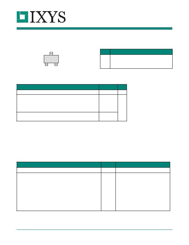
1.1 Package Pinout
1.2 Pin Description
1.3 Absolute Maximum Ratings
Absolute maximum electrical ratings are at 25癈.
Absolute maximum ratings are stress ratings.
Stresses in excess of these ratings can cause
permanent damage to the device. Functional
operation of the device at conditions beyond those
indicated in the operational sections of this data sheet
is not implied.
1.4 Electrical Characteristics
Over operating voltage and temperature range unless otherwise specified.
Notes: 1. B
OPX
= operating point (output turns ON); B
RPX
= release point (output turns OFF).
2. Typical data is at 25癈 and V
SUPPLY
= 3V.
1
2
3
Pin#
Name
Description
1
V
SUPPLY 2.5V to 5.5V
2
OUT
Open-Drain, N-Channel FET
3
GROUND
Ground
Parameter
Symbol
Min
Max
Units
Supply Voltage
V
SUPPLY
-0.5
6
V
DC
Output Voltage
V
OUT
-0.5
6
V
Magnetic Flux Density
B
-
Unlimited
G
Output Current
I
OUT
-
5
mA
Junction Temperature
T
J
-
150
癈
Operating Ambient Temperature
T
A
-40
85
Storage Temperature
T
STG
-40
150
Parameter
Conditions
Symbol
Minimum
Typical
Maximum
Units
Supply Voltage Range
Operating
V
SUPPLY
2.5
-
5.5
V
DC
Output Leakage Current
V
OUT
=5.5V, B
RPN
< B < B
RPS
I
LKG
-
-
1
mA
Output On Voltage
I
OUT
=1mA, V
DD
=3.0V
V
OUT
-
100
300
mV
Awake Time
-
-
-
-
90
ms
Period
-
-
-
-
90
ms
Duty Cycle
-
-
-
0.1
-
%
Supply Current
Awake (enabled)
I
SUPPLY
-
-
2
mA
Asleep (disabled)
-
-
8
mA
Average (Calculated)
-
5
15
mA
發布緊急采購,3分鐘左右您將得到回復。