- 您現在的位置:買賣IC網 > PDF目錄382345 > MPC9448 (Motorola, Inc.) 3.3V/2.5V LVCMOS 1:12 Clock Fanout Buffer PDF資料下載
參數資料
| 型號: | MPC9448 |
| 廠商: | Motorola, Inc. |
| 英文描述: | 3.3V/2.5V LVCMOS 1:12 Clock Fanout Buffer |
| 中文描述: | 3.3V/2.5V的LVCMOS 1:12時鐘扇出緩沖器 |
| 文件頁數: | 6/12頁 |
| 文件大小: | 263K |
| 代理商: | MPC9448 |
MPC9448
MOTOROLA
TIMING SOLUTIONS
6
APPLICATIONS INFORMATION
Figure 3. Output Clock Stop (CLK_STOP) Timing
Diagram
CCLK or
PCLK
CLK_STOP
Q0 to Q11
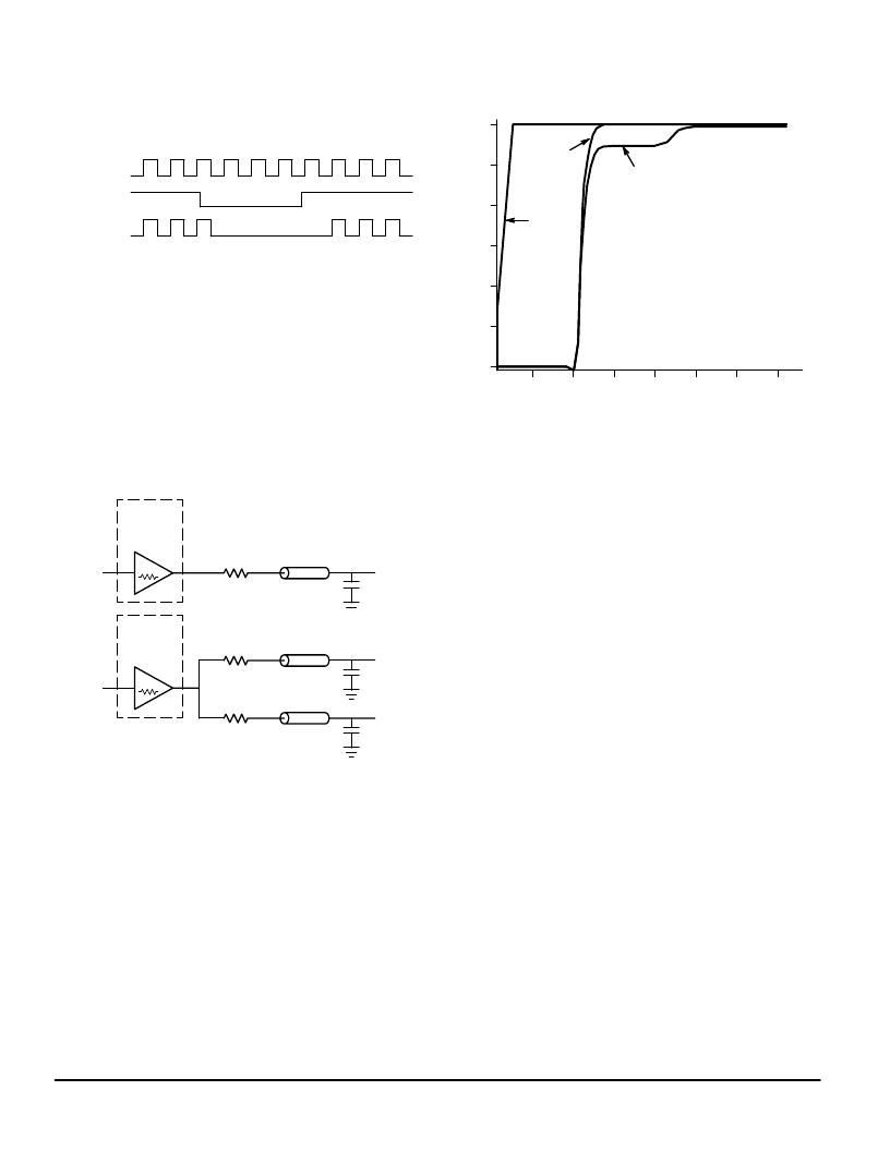
Driving Transmission Lines
The MPC9448 clock driver was designed to drive high
speed signals in a terminated transmission line environment.
To provide the optimum flexibility to the user, the output
drivers were designed to exhibit the lowest impedance
possible. With an output impedance of 17
(V
CC
=3.3V), the
outputs can drive either parallel or series terminated
transmission lines.
For more information on transmission
lines, the reader is referred to Motorola application note
AN1091.
In most high performance clock networks,
point--to--point distribution of signals is the method of choice.
In a point--to--point scheme, either series terminated or
parallel terminated transmission lines can be used.
parallel technique terminates the signal at the end of the line
with a 50
resistance to V
CC
÷
2.
The
Figure 4. Single versus Dual Transmission Lines
This technique draws a fairly high level of DC current and
thus only a single terminated line can be driven by each
output of the MPC9448 clock driver.
terminated case, however, there is no DC current draw; thus,
the outputs can drive multiple series terminated lines.
Figure 4 “Single versus Dual Transmission Lines” illustrates
an output driving a single series terminated line versus two
series terminated lines in parallel. When taken to its extreme,
the fanout of the MPC9448 clock driver is effectively doubled
due to its capability to drive multiple lines at V
CC
=3.3V.
17
IN
MPC9448
OUTPUT
BUFFER
R
S
= 33
Z
O
= 50
OutA
17
IN
MPC9448
OUTPUT
BUFFER
R
S
= 33
Z
O
= 50
OutB0
R
S
= 33
Z
O
= 50
OutB1
For the series
Figure 5. Single versus Dual Line Termination
Waveforms
TIME (nS)
V
3.0
2.5
2.0
1.5
1.0
0.5
0
2
4
6
8
10
12
14
OutB
t
D
= 3.9386
OutA
t
D
= 3.8956
In
The waveform plots in Figure 5 “Single versus Dual Line
Termination Waveforms” show the simulation results of an
output driving a single line versus two lines. In both cases,
the drive capability of the MPC9448 output buffer is more
than sufficient to drive 50
transmission lines on the incident
edge. Note from the delay measurements in the simulations
a delta of only 43ps exists between the two differently loaded
outputs. This suggests that the dual line driving need not be
used exclusively to maintain the tight output--to--output skew
of the MPC9448. The output waveform in Figure 5 “Single
versus Dual Line Termination Waveforms” shows a step in
the waveform; this step is caused by the impedance
mismatch seen looking into the driver. The parallel
combination of the 33
series resistor plus the output
impedance does not match the parallel combination of the
line impedances. The voltage wave launched down the two
lines will equal:
V
L
= V
S
( Z
0
÷
(R
S
+R
0
+Z
0
))
Z
0
= 50
|| 50
R
S
= 33
|| 33
R
0
= 17
V
L
= 3.0 ( 25
÷
(16.5+17+25)
= 1.28V
At the load end the voltage will double, due to the near
unity reflection coefficient, to 2.5V.
towards the quiescent 3.0V in steps separated by one round
trip delay (in this case 4.0ns).
It will then increment
F
Freescale Semiconductor, Inc.
For More Information On This Product,
Go to: www.freescale.com
n
.
相關PDF資料 |
PDF描述 |
|---|---|
| MPC9448D | 3.3V/2.5V LVCMOS 1:12 Clock Fanout Buffer |
| MPC9600 | LOW VOLTAGE 2.5 V AND 3.3 V CMOS PLL CLOCK DRIVER |
| MPC9772 | 3.3V 1:12 LVCMOS PLL Clock Generator |
| MPC9893 | Low Voltage PLL Intelligent Dynamic Clock (IDCS) Switch |
| MPC99J93 | Intelligent Dynamic Clock Switch (IDCS) PLL Clock Driver |
相關代理商/技術參數 |
參數描述 |
|---|---|
| MPC9448AC | 功能描述:時鐘緩沖器 3.3V 900MHz Clock Generator RoHS:否 制造商:Texas Instruments 輸出端數量:5 最大輸入頻率:40 MHz 傳播延遲(最大值): 電源電壓-最大:3.45 V 電源電壓-最小:2.375 V 最大功率耗散: 最大工作溫度:+ 85 C 最小工作溫度:- 40 C 封裝 / 箱體:LLP-24 封裝:Reel |
| MPC9448ACR2 | 功能描述:時鐘緩沖器 FSL 1-12 LVCMOS Fanout Buffer RoHS:否 制造商:Texas Instruments 輸出端數量:5 最大輸入頻率:40 MHz 傳播延遲(最大值): 電源電壓-最大:3.45 V 電源電壓-最小:2.375 V 最大功率耗散: 最大工作溫度:+ 85 C 最小工作溫度:- 40 C 封裝 / 箱體:LLP-24 封裝:Reel |
| MPC9448D | 制造商:MOTOROLA 制造商全稱:Motorola, Inc 功能描述:3.3V/2.5V LVCMOS 1:12 Clock Fanout Buffer |
| MPC9448FA | 功能描述:時鐘緩沖器 2.5 3.3V 275MHz Clock Generator RoHS:否 制造商:Texas Instruments 輸出端數量:5 最大輸入頻率:40 MHz 傳播延遲(最大值): 電源電壓-最大:3.45 V 電源電壓-最小:2.375 V 最大功率耗散: 最大工作溫度:+ 85 C 最小工作溫度:- 40 C 封裝 / 箱體:LLP-24 封裝:Reel |
| MPC9448FAR2 | 功能描述:IC CLOCK BUFFER MUX 2:12 32-LQFP RoHS:否 類別:集成電路 (IC) >> 時鐘/計時 - 時鐘緩沖器,驅動器 系列:- 標準包裝:1 系列:HiPerClockS™ 類型:扇出緩沖器(分配),多路復用器 電路數:1 比率 - 輸入:輸出:2:18 差分 - 輸入:輸出:是/無 輸入:CML,LVCMOS,LVPECL,LVTTL,SSTL 輸出:LVCMOS,LVTTL 頻率 - 最大:250MHz 電源電壓:2.375 V ~ 3.465 V 工作溫度:0°C ~ 70°C 安裝類型:表面貼裝 封裝/外殼:32-LQFP 供應商設備封裝:32-TQFP(7x7) 包裝:- 其它名稱:800-1923-6 |
發布緊急采購,3分鐘左右您將得到回復。