- 您現在的位置:買賣IC網 > PDF目錄382333 > MM54HC42 (National Semiconductor Corporation) BCD-to-Decimal Decoder PDF資料下載
參數資料
| 型號: | MM54HC42 |
| 廠商: | National Semiconductor Corporation |
| 英文描述: | BCD-to-Decimal Decoder |
| 中文描述: | BCD碼到十進制解碼器 |
| 文件頁數: | 1/4頁 |
| 文件大小: | 149K |
| 代理商: | MM54HC42 |
TL/F/5301
M
January 1988
MM54HC42/MM74HC42
BCD-to-Decimal Decoder
General Description
This decoder utilizes advanced silicon-gate CMOS technol-
ogy. Data on the four input pins select one of the 10 outputs
corresponding to the value of the BCD number on the in-
puts. An output will go low when selected, otherwise it re-
mains high. If the input data is not a valid BCD number all
outputs will remain high. The circuit has high noise immunity
and low power consumption usually associated with CMOS
circuitry, yet also has speeds comparable to low power
Schottky TTL (LS-TTL) circuits, and is capable of driving 10
LS-TTL equivalent loads.
All inputs are protected from damage due to static dis-
charge by diodes to V
CC
and ground.
Features
Y
Typical propagation delay: 15 ns
Y
Wide supply range: 2V–6V
Y
Low quiescent current: 80
m
A (74HC)
Y
Fanout of 10 LS-TTL loads
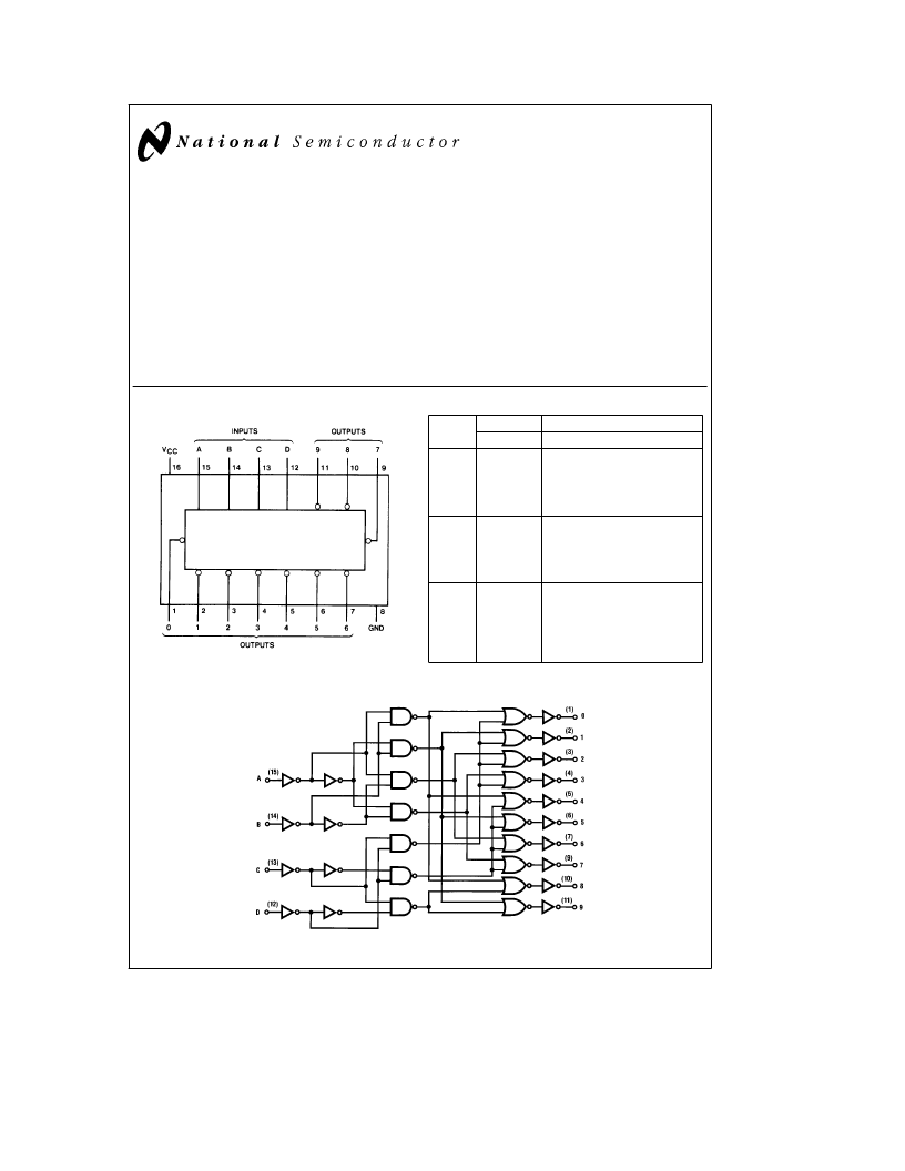
Connection Diagram
Dual-in-line Package
TL/F/5301–1
Top View
Order Number MM54HC42 or MM74HC42
Logic Diagram
Truth Table
No.
Inputs
D C B A
L
L
L
L
L
L
L
L
L
H
L
H
L
H H
L
H H H H H H H H H H
H
L
L
L
H H H H H H H H
H
L
L
H H H H H H H H H H
H
L
H
L
H H H H H H H H H H
H
L
H H H H H H H H H H H H
H H
L
L
H H H H H H H H H H
H H
L
H H H H H H H H H H H
H H H
L
H H H H H H H H H H
H H H H H H H H H H H H H H
Outputs
4
0
L
1
H H H H H H H H H
L
H H H H H H H H
H H
L
H H H H H H H
H H H H H
L
L
L
H H H H
L
H H H H H H
L
H H H H H H
2
3
5
6
7
8
9
0
1
2
3
4
5
6
7
8
9
L
L
H
L
H H
L
H H H H H H
L
H H H H H
L
H H H H
L
H H H
L
H H
L
H
L
INVALID
H
e
High Level, L
e
Low Level
TL/F/5301–2
C
1995 National Semiconductor Corporation
RRD-B30M105/Printed in U. S. A.
相關PDF資料 |
PDF描述 |
|---|---|
| MM54HC42J | BCD-to-Decimal Decoder |
| MM54HC42N | BCD-to-Decimal Decoder |
| MM74HC42 | BCD-to-Decimal Decoder |
| MM54HC640 | Inverting Octal TRI-STATE Transceiver |
| MM54HC640J | Inverting Octal TRI-STATE Transceiver |
相關代理商/技術參數 |
參數描述 |
|---|---|
| MM54HC423 WAF | 制造商:Texas Instruments 功能描述: |
| MM54HC42E/883 | 制造商:Rochester Electronics LLC 功能描述:- Bulk 制造商:Texas Instruments 功能描述: |
| MM54HC42J | 制造商:NSC 制造商全稱:National Semiconductor 功能描述:BCD-to-Decimal Decoder |
| MM54HC42N | 制造商:NSC 制造商全稱:National Semiconductor 功能描述:BCD-to-Decimal Decoder |
| MM54HC4511 | 制造商:NSC 制造商全稱:National Semiconductor 功能描述:BCD-to-7 Segment Latch/Decoder/Driver |
發布緊急采購,3分鐘左右您將得到回復。