- 您現(xiàn)在的位置:買(mǎi)賣(mài)IC網(wǎng) > PDF目錄382315 > MC74VHCT02ADT (ON SEMICONDUCTOR) Quad 2-Input NOR Gate PDF資料下載
參數(shù)資料
| 型號(hào): | MC74VHCT02ADT |
| 廠(chǎng)商: | ON SEMICONDUCTOR |
| 元件分類(lèi): | 通用總線(xiàn)功能 |
| 英文描述: | Quad 2-Input NOR Gate |
| 中文描述: | AHCT/VHCT SERIES, QUAD 2-INPUT NOR GATE, PDSO14 |
| 封裝: | TSSOP-14 |
| 文件頁(yè)數(shù): | 3/8頁(yè) |
| 文件大小: | 145K |
| 代理商: | MC74VHCT02ADT |
MC74VHCT02A
VHC Data – Advanced CMOS Logic
DL203 — Rev 1
3
MOTOROLA
b l
di i
tPLH,
tPHL
Input A or B to Y
C, VCC = 5.0V
U i
8.1
11.4
13.0
9.5
17.5
12.5
ns
5.1
7.5
8.5
11.0
Cin
Maximum Input Capacitance
4
10
10
10
pF
CPD
Power Dissipation Capacitance (Note 1.)
1 )
20
pF
1. CPD is defined as the value of the internal equivalent capacitance which is calculated from the operating current consumption without load.
Average operating current can be obtained by the equation: ICC(OPR
)
= CPD VCC fin + ICC/4 (per gate). CPD s used to determine the no–load
dynamic power consumption; PD = CPD VCC2 fin + ICC VCC.
NOISE CHARACTERISTICS
(Input tr = tf = 3.0ns, CL = 50pF, VCC = 5.0V)
Symbol
b l
Characteristic
i i
TA = 25
°
C
Typ
U i
Unit
Max
VOLP
VOLV
VIHD
VILD
Quiet Output Maximum Dynamic VOL
Quiet Output Minimum Dynamic VOL
Minimum High Level Dynamic Input Voltage
0.3
0.8
V
– 0.3
– 0.8
V
3.5
V
Maximum Low Level Dynamic Input Voltage
1.5
V
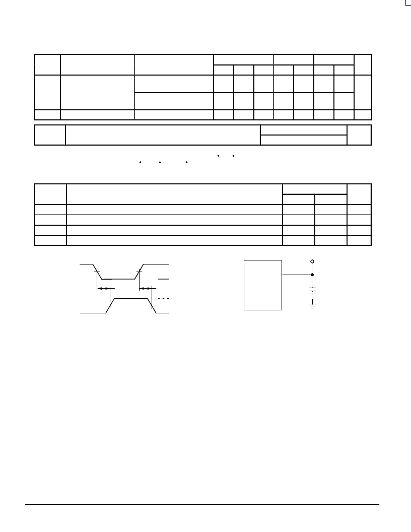
Figure 1. Switching Waveforms
3.0V
GND
1.5V
1.5V
A or B
Y
tPHL
tPLH
* Includes all probe and jig capacitance
Figure 2. Test Circuit
CL*
TEST POINT
DEVICE
UNDER
TEST
OUTPUT
VOH
VOL
發(fā)布緊急采購(gòu),3分鐘左右您將得到回復(fù)。