- 您現在的位置:買賣IC網 > PDF目錄375864 > FMS6501MSA28X (FAIRCHILD SEMICONDUCTOR CORP) 12 Input 9 Output Video Switch Matrix with Input Clamp, Input Bias Circuitry, and Output Drivers PDF資料下載
參數資料
| 型號: | FMS6501MSA28X |
| 廠商: | FAIRCHILD SEMICONDUCTOR CORP |
| 元件分類: | 運動控制電子 |
| 英文描述: | 12 Input 9 Output Video Switch Matrix with Input Clamp, Input Bias Circuitry, and Output Drivers |
| 中文描述: | 12-CHANNEL, AUDIO/VIDEO SWITCH, PDSO28 |
| 封裝: | LEAD FREE, SSOP-28 |
| 文件頁數: | 6/16頁 |
| 文件大小: | 166K |
| 代理商: | FMS6501MSA28X |
6
www.fairchildsemi.com
FMS6501 Rev. 1A
F
I
2
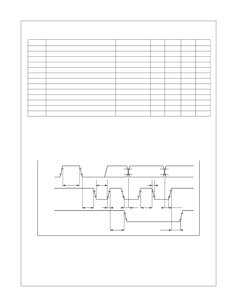
C BUS Characteristics
T
c
= 25°C, V
cc
= 5V; unless otherwise noted.
Symbol
Digital Input Low
1
Digital Input High
1
Notes:
1. 100% tested at 25°C
Figure 1: I
2
C Bus Timing
Parameter
Conditions
Min.
Typ.
Max
Units
V
il
V
ih
f
scl
tr
SDA, SCL, ADDR
0
1.5
V
cc
V
SDA, SCL, ADDR
3.0
V
Clock Frequency
SCK
100
kHz
Input Rise Time
1.5V to 3V
1000
nS
tf
Input Fall Time
1.5V to 3V
300
nS
t
low
t
high
t
SU,DAT
t
HD,DAT
t
SU,STO
t
BUF
t
HD,STA
t
SU,STA
Clock Low Period
4.7
uS
Clock High Period
4.0
uS
Data Set-up Time
300
nS
Data Hold Time
0
nS
Set-up Time from Clock High to Stop
4
uS
Start Set-up Time following a Stop
4.7
uS
Start Hold Time
4
uS
Start Set-up Time following Clock Low to High
4.7
uS
SDA
SCL
SDA
tBUF
tLOW
tf
tHD,STA
tr
tHD,DAT
tHIGH
tSU,DAT
tSU,STO
tSU,STA
相關PDF資料 |
PDF描述 |
|---|---|
| FMS6690 | Six Channel, 6th Order SD/PS/HD Video Filter Driver |
| FMS6690MTC20X | Six Channel, 6th Order SD/PS/HD Video Filter Driver |
| FMS6G10US60S | Compact & Complex Module |
| FMS6G15US60S | Compact & Complex Module |
| FMS6G15US60 | Compact & Complex Module |
相關代理商/技術參數 |
參數描述 |
|---|---|
| FMS6502 | 制造商:FAIRCHILD 制造商全稱:Fairchild Semiconductor 功能描述:8-Input, 6-Output Video Switch Matrix with Output Drivers, Input Clamp, and Bias Circuitry |
| FMS6502MTC24 | 功能描述:視頻 IC 8/6 I/O Video Switch Matrix Output Driver RoHS:否 制造商:Fairchild Semiconductor 工作電源電壓:5 V 電源電流:80 mA 最大工作溫度:+ 85 C 封裝 / 箱體:TSSOP-28 封裝:Reel |
| FMS6502MTC24X | 功能描述:視頻 IC Switch Video 8I 6O Matrix-Output Dvrs RoHS:否 制造商:Fairchild Semiconductor 工作電源電壓:5 V 電源電流:80 mA 最大工作溫度:+ 85 C 封裝 / 箱體:TSSOP-28 封裝:Reel |
| FMS6601_AAA3026B WAF | 制造商:Fairchild Semiconductor Corporation 功能描述: |
| FMS6646 | 制造商:FAIRCHILD 制造商全稱:Fairchild Semiconductor 功能描述:Six Channel, SD/HD (1080p) Video Filter Driver |
發布緊急采購,3分鐘左右您將得到回復。