- 您現在的位置:買賣IC網 > PDF目錄375860 > FMM5815X (SUMITOMO ELECTRIC DEVICE INNOVATIONS, INC.) 17.5-20GHz Power Amplifier MMIC PDF資料下載
參數資料
| 型號: | FMM5815X |
| 廠商: | SUMITOMO ELECTRIC DEVICE INNOVATIONS, INC. |
| 英文描述: | 17.5-20GHz Power Amplifier MMIC |
| 中文描述: | 17.5 - 20GHz的功率放大器單片 |
| 文件頁數: | 1/4頁 |
| 文件大小: | 231K |
| 代理商: | FMM5815X |
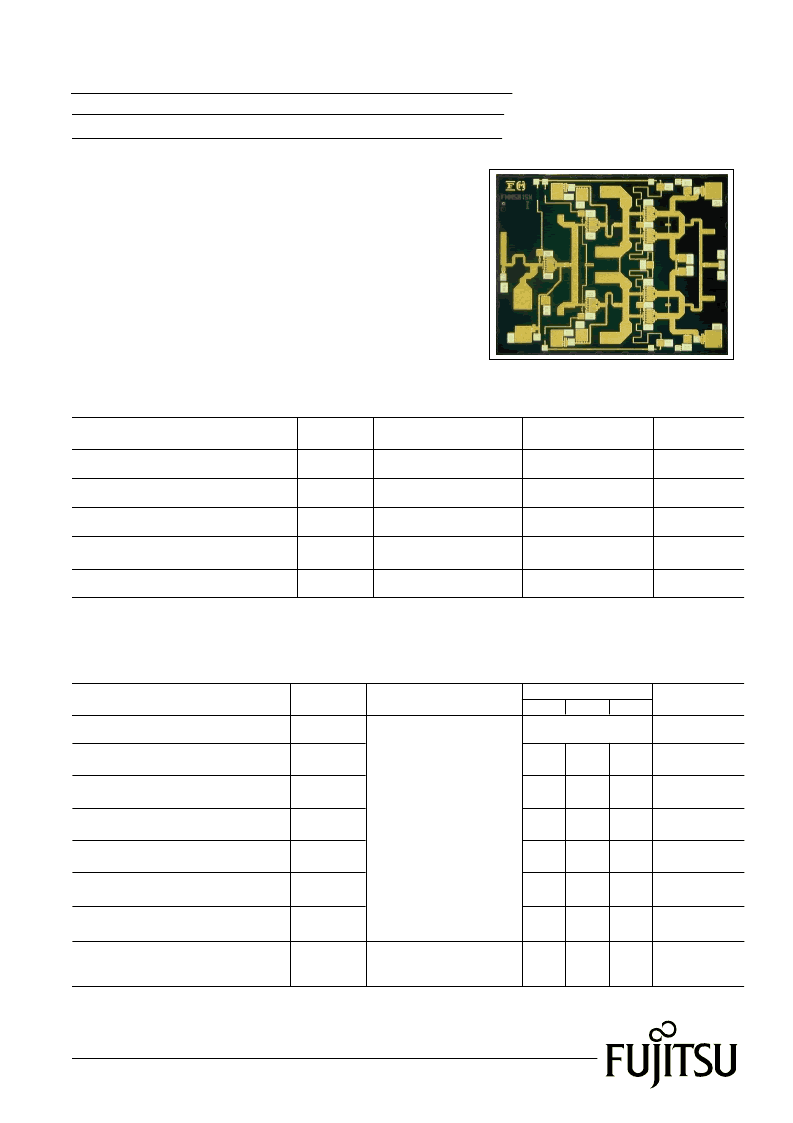
FMM5815X
17.5-20GHz Power Amplifier MMIC
Item
Symbol
Drain Voltage
VDD
10
V
Gate Voltage
VGG
-3.0
V
Input Power
Pin
22
dBm
°
C
Storage Temperature
-65 to +175
Tstg
Condition
Unit
Rating
ABSOLUTE MAXIMUM RATING (Ambient Temperature Ta=25
°
C)
Fujitsu recommends the following conditions for the long term reliable operation of GaAs FETs:
1. The drain-source operating voltage (VDD) should not exceed 6 volts.
2. The forward and reverse gate currents should not exceed 4 and -0.39 mA respectively.
3. This product should be hermetically packaged
Operating Backside Temperature
-65 to +85
°
C
Top
1
Edition 1.0
June 2001
Item
Symbol
Output Return Loss
RLout
Conditions
Unit
Limits
Typ.
17.5 - 20.0
Max.
Min.
ELECTRICAL CHARACTERISTICS (Ambient Temperature Tc=25
°
C)
Power Gain at 1 dB G.C.P.
19
21
24
-
-8
-
dB
-
700
950
mA
Input Return Loss
RLin
Iddrf
-
-
-12
dB
dB
3rd Order Intermodulation
Distortion
IM3
-
-40
-37.0
dBc
Frequency Range
f
GHz
Output Power at 1 dB G.C.P.
29.5
31
-
dBm
P
1dB
G
1dB
G.C.P.: Gain Compression Point
S.C.L.: Single Carrier Level
Power-Added Efficiency
Drain Current
-
30
-
%
η
add
VDD = 6V
IDD
=
600mA (Typ.)
ZS = ZL = 50
f=10MHz, 2-Tone Test,
Pout=20dBm S.C.L.
Note 2:
Electrical Characteristic is specified on RF-probe measurements
Note 1:
RF parameter sample size 10pcs. Criteria (accept/reject)=(0/1)
DESCRIPTION
The FMM5815X is a high-gain, high linearity, 3-stage MMIC
amplifier designed for operation in the17.5-20.0 GHz
frequency range. This amplifier has an input and output
designed for use in 50
systems.This device is well suited
for point-to-point communication applications.
FEATURES
High Output Power: P1dB= 31dBm (Typ.)
High Gain: G1dB= 21dB (Typ.)
High PAE:
η
add= 30% (Typ.)
Impedance Matched Zin/Zout = 50
0.25μm PHEMT Technology
相關PDF資料 |
PDF描述 |
|---|---|
| FMM5820QH | Ka-Band Power Amplifier MMIC |
| FMM5820X | Ka-Band Power Amplifier MMIC |
| FMM5822X | K-Band Power Amplifier MMIC |
| FMM5823X | K-Band Power Amplifier MMIC |
| FMM5826X | Ka-Band Power Amplifier MMIC |
相關代理商/技術參數 |
參數描述 |
|---|---|
| FMM5820QH | 制造商:EUDYNA 制造商全稱:Eudyna Devices Inc 功能描述:Ka-Band Power Amplifier MMIC |
| FMM5820X | 制造商:EUDYNA 制造商全稱:Eudyna Devices Inc 功能描述:Ka-Band Power Amplifier MMIC |
| FMM5822VU | 制造商:SUMITOMO ELECTRIC Device Innovations Inc 功能描述:C to Ka-Band, Power Amplifier MMIC, 17.7-19.7GHz, 32dBm, 1100mA, Bulk |
| FMM5822X | 制造商:EUDYNA 制造商全稱:Eudyna Devices Inc 功能描述:K-Band Power Amplifier MMIC |
| FMM5823X | 制造商:EUDYNA 制造商全稱:Eudyna Devices Inc 功能描述:K-Band Power Amplifier MMIC |
發布緊急采購,3分鐘左右您將得到回復。