- 您現在的位置:買賣IC網 > PDF目錄375846 > FM24C32UTHM8 (FAIRCHILD SEMICONDUCTOR CORP) EEPROM PDF資料下載
參數資料
| 型號: | FM24C32UTHM8 |
| 廠商: | FAIRCHILD SEMICONDUCTOR CORP |
| 元件分類: | DRAM |
| 英文描述: | EEPROM |
| 中文描述: | 4K X 8 I2C/2-WIRE SERIAL EEPROM, PDSO8 |
| 封裝: | SOIC-8 |
| 文件頁數: | 6/13頁 |
| 文件大小: | 85K |
| 代理商: | FM24C32UTHM8 |
6
www.fairchildsemi.com
FM24C32U Rev. A.1
F
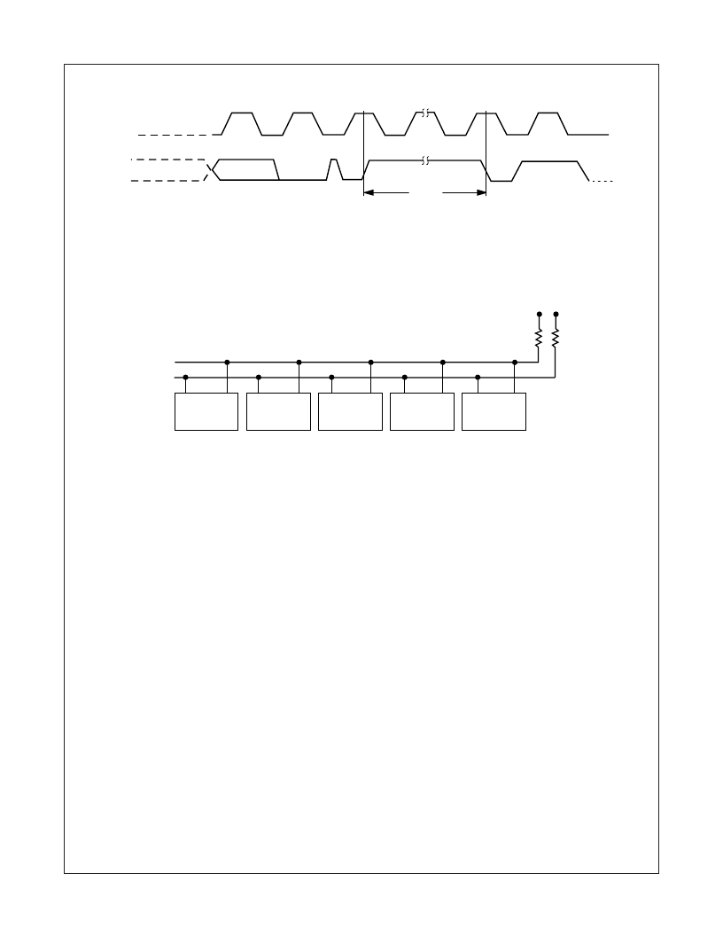
SDA
SCL
Master
Transmitter/
Receiver
Slave
Transmitter/
Receiver
Master
Transmitter
Slave
Receiver
Master
Transmitter/
Receiver
V
CC
V
CC
Typical System Configuration
Note:
Due to open drain configuration of SDA and SCL, a bus-level pull-up resistor is called for, (typical value = 4.7k
)
SDA
SCL
STOP
CONDITION
START
CONDITION
WORD n
8th BIT
ACK
tWR
Write Cycle Timing
Note:
The write cycle time (t
WR
) is the time from a valid stop condition of a write sequence to the end of the internal erase/program cycle.
發布緊急采購,3分鐘左右您將得到回復。