- 您現在的位置:買賣IC網 > PDF目錄373969 > AD9854 (Analog Devices, Inc.) CMOS 300MHz Quadrature Complete-DDS PDF資料下載
參數資料
| 型號: | AD9854 |
| 廠商: | Analog Devices, Inc. |
| 元件分類: | XO, clock |
| 英文描述: | CMOS 300MHz Quadrature Complete-DDS |
| 中文描述: | 300MHz CMOS正交DDS數字合成器 |
| 文件頁數: | 22/28頁 |
| 文件大小: | 589K |
| 代理商: | AD9854 |
第1頁第2頁第3頁第4頁第5頁第6頁第7頁第8頁第9頁第10頁第11頁第12頁第13頁第14頁第15頁第16頁第17頁第18頁第19頁第20頁第21頁當前第22頁第23頁第24頁第25頁第26頁第27頁第28頁
AD9854 PRELIMINARY TECHNICAL DATA
_____________________________________________________________________________________________________
General Operation of the Serial Interface
7/16/99 REV.PRA
22
There are two phases to a communication cycle with the
AD9854/52. Phase 1 is the instruction cycle, which is the
writing of an instruction byte into the AD9854/52,
coincident with the first 8 SCLK rising edges. The
instruction byte provides the AD9854/52 serial port
controller with information regarding the data transfer
cycle, which is phase 2 of the communication cycle. The
Phase 1 instruction byte defines whether the upcoming data
transfer is read or write, and
the register address in which
to transfer data to/from.
The first eight SCLK rising edges of each communication
cycle are used to write the instruction byte into the
AD9854/52. The remaining SCLK edges are for phase 2 of
the communication cycle. Phase 2 is the actual data
transfer between the AD9854/52 and the system controller.
The number of data bytes transferred in Phase 2 of the
communication cycle is a function of the register address.
The AD9854/52 internal serial IO controller expects every
byte of the register being accessed to be transferred. Table
below describes how many bytes must be transferred
Serial Register
Address
0
1
2
3
4
5
6
7
8
9
A
B
Register Name
Phase OffsetTuning Word Register#1
Phase OffsetTuning Word Register #2
Frequency Tuning Word #1
Frequency Tuning Word #2
Delta FrequencyRegister
Update Clock Rate Register
Ramp Rate Clock Register
Control Register
I Path Digital Multiplier Register
Q Path Digital Multiplier Register
Shaped On-Off Keying Ramp Rate Register
Q DAC Register
Number of Bytes
Transferred
2 bytes
2 bytes
6 bytes
6 bytes
6 bytes
4 bytes
3 bytes
4 bytes
2 bytes
2 bytes
2 bytes
2 bytes
At the completion of any communication cycle, the
AD9854/52 serial port controller expects the next 8 rising
SCLK edges to be the instruction byte of the next
communication cycle. In addition, an active high input on
the IORESET pin immediately terminates the current
communication cycle. After IORESET returns low, the
AD9854/52 serial port controller requires the next 8 rising
SCLK edges to be the instruction byte of the next
communication cycle.
All data input to the AD9854/52 is registered on the rising
edge of SCLK. All data is driven out of the AD9854/52 on
the falling edge of SCLK.
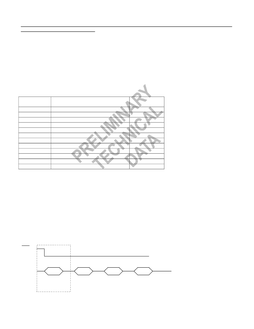
Figures 2 and 3 are useful in understanding the general
operation of the AD9854/52 Serial Port.
Figure 2. Using SDIO as a Read/Write Transfer
SDIO
CS
INSTRUCTION
BYTE
DATA BYTE 1
DATA BYTE 2
DATA BYTE 3
DATA TRANSFER
INSTRUCTION
CYCLE
相關PDF資料 |
PDF描述 |
|---|---|
| AD9858TLPCB | 1 GSPS Direct Digital Synthesizer |
| AD9858BSV | 1 GSPS Direct Digital Synthesizer |
| AD9858PCB | 1 GSPS Direct Digital Synthesizer |
| AD9858 | 1 GSPS Direct Digital Synthesizer |
| AD9858FDPCB | 1 GSPS Direct Digital Synthesizer |
相關代理商/技術參數 |
參數描述 |
|---|---|
| AD9854/PCB | 制造商:Analog Devices 功能描述:Evaluation Board For IC Digital Synthesizer Single 制造商:Analog Devices 功能描述:Direct Digital Synthesizer IC (DDS) |
| AD9854/PCBZ | 功能描述:BOARD EVAL FOR AD9854 RoHS:是 類別:編程器,開發系統 >> 評估演示板和套件 系列:AgileRF™ 標準包裝:1 系列:PCI Express® (PCIe) 主要目的:接口,收發器,PCI Express 嵌入式:- 已用 IC / 零件:DS80PCI800 主要屬性:- 次要屬性:- 已供物品:板 |
| AD9854ASQ | 制造商:Analog Devices 功能描述:IC DDS SYNTHESIZER |
| AD9854ASQZ | 制造商:Analog Devices 功能描述:Direct Digital Synthesizer 300MHz 2-DAC 12-Bit Parallel/Serial 80-Pin LQFP 制造商:Analog Devices 功能描述:Communication IC |
| AD9854AST | 制造商:Analog Devices 功能描述:Direct Digital Synthesizer 300MHz 2-DAC 12-Bit Parallel/Serial 80-Pin LQFP Tray 制造商:Rochester Electronics LLC 功能描述:200 MHZ QUADRATURE DDS SYNTHESIZER - Tape and Reel 制造商:Analog Devices 功能描述:IC SEMICONDUCTOR ((NS)) |
發布緊急采購,3分鐘左右您將得到回復。