- 您現在的位置:買賣IC網 > PDF目錄373929 > AD8017 (Analog Devices, Inc.) Dual High Output Current, High Speed Amplifier PDF資料下載
參數資料
| 型號: | AD8017 |
| 廠商: | Analog Devices, Inc. |
| 元件分類: | 運動控制電子 |
| 英文描述: | Dual High Output Current, High Speed Amplifier |
| 中文描述: | 雙路高輸出電流,高速放大器 |
| 文件頁數: | 15/16頁 |
| 文件大小: | 223K |
| 代理商: | AD8017 |
AD8017
–15–
REV. A
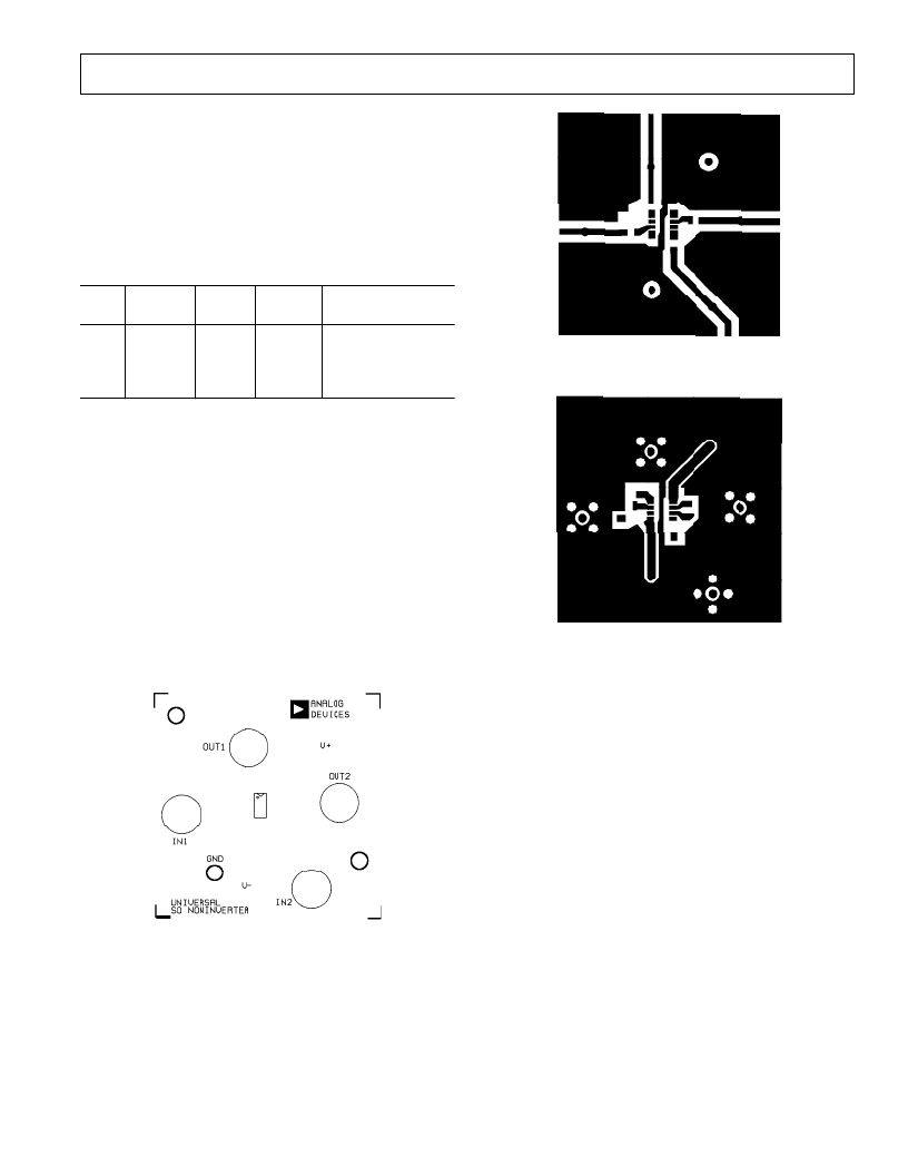
LAYOUT CONSIDERATIONS
The specified high speed performance of the AD8017 requires
careful attention to board layout and component selection.
Table II shows recommended component values for the AD8017
and Figures 42
–
44 show recommended layouts for the 8-lead
SOIC package for a positive gain. Proper RF design techniques
and low parasitic component selections are mandatory.
Table II. Typical Bandwidth vs. Gain Setting Resistors
(V
S
= 6 V, R
L
= 100 )
Small Signal
–3 dB BW (MHz)
Gain
R
F
( )
619
619
619
619
R
G
( )
619
R
T
( )
54.5
49.9
49.9
49.9
–
1
+1
+2
+10
110
320
160
40
619
68.8
R
T
chosen for 50
characteristic input impedance.
The PCB should have a ground plane covering all unused
portions of the component side of the board to provide a low
impedance ground path. The ground plane should be removed
from the area near the input pins to reduce stray capacitance.
Chip capacitors should be used for supply bypassing (see Fig-
ures 4 and 7). One end should be connected to the ground
plane and the other within 1/8 in. of each power pin. An addi-
tional (4.7
μ
F
–
10
μ
F) tantalum electrolytic capacitor should be
connected in parallel.
The feedback resistor should be located close to the inverting
input pin in order to keep the stray capacitance at this node to
a minimum. Capacitance greater than 1.5 pF at the inverting
input will significantly affect high speed performance when
operating at low noninverting gain.
Figure 42. Universal SOIC Noninverter Top Silkscreen
Figure 43. Universal SOIC Noninverter Top
Figure 44. Universal SOIC Noninverter Bottom
相關PDF資料 |
PDF描述 |
|---|---|
| AD8017AR | Dual High Output Current, High Speed Amplifier |
| AD8017AR-EVAL | Dual High Output Current, High Speed Amplifier |
| AD8017AR-REEL | Dual High Output Current, High Speed Amplifier |
| AD8017AR-REEL7 | Dual High Output Current, High Speed Amplifier |
| AD8018ARU-EVAL | 5 V, Rail-to-Rail, High-Output Current, xDSL Line Drive Amplifier |
相關代理商/技術參數 |
參數描述 |
|---|---|
| AD8017_02 | 制造商:AD 制造商全稱:Analog Devices 功能描述:Dual High Output Current, High Speed Amplifier |
| AD80172 | 制造商:Analog Devices 功能描述: |
| AD80175-1 | 制造商:Analog Devices 功能描述: |
| AD80175-2 | 制造商:Analog Devices 功能描述: |
| AD80176YSVZ | 制造商:Analog Devices 功能描述:- Rail/Tube |
發布緊急采購,3分鐘左右您將得到回復。