- 您現在的位置:買賣IC網 > PDF目錄373924 > AD7892SQ (Analog Devices, Inc.) Dual High Efficiency, Low Noise, Synchronous Step-Down Switching Regulators PDF資料下載
參數資料
| 型號: | AD7892SQ |
| 廠商: | Analog Devices, Inc. |
| 元件分類: | 基準電壓源/電流源 |
| 英文描述: | Dual High Efficiency, Low Noise, Synchronous Step-Down Switching Regulators |
| 中文描述: | 雙通道高效率,低噪聲,同步降壓型開關穩壓器 |
| 文件頁數: | 7/14頁 |
| 文件大小: | 144K |
| 代理商: | AD7892SQ |
AD7892
REV. C
–7–
Pin
No.
Mnemonic
Description
16
DB4/SCLK
Data Bit 4/Serial Clock. When the device is in its parallel mode, this pin is Data Bit 4, a three-state
TTL-compatible output. When the device is in its serial mode, this becomes the serial clock pin,
SCLK. SCLK is an input and an external serial clock must be provided at this pin to obtain serial
data from the AD7892. Serial data is clocked out from the output shift register on the rising edges
of SCLK after
RFS
goes low.
Data Bit 3/Receive Frame Synchronization. When the device is in its parallel mode, this pin is Data
Bit 3, a three-state TTL-compatible output. When the device is in its serial mode, this becomes the
receive frame synchronization input with
RFS
provided externally to obtain serial data from the
AD7892.
Data Bit 2. Three-state TTL-compatible output. This output should be left unconnected when the
device is in its serial mode.
Data Bit 1. Three-state TTL-compatible output. This output should be left unconnected when the
device is in its serial mode.
Data Bit 0 (LSB). Three-state TTL-compatible output. Output coding is two’s complement for
AD7892-1 and AD7892-3 and straight (natural) binary for AD7892-2. This output should be left
unconnected when the device is in its serial mode.
Read. Active low logic input which is used in conjunction with
CS
low to enable the data outputs.
Chip Select. Active low logic input which is used in conjunction with
RD
to enable the data outputs.
End-of-Conversion. Active low logic output indicating converter status. The end of conversion is
signified by a low going pulse on this line. The duration of this
EOC
pulse is nominally 100 ns.
Convert Start. Logic Input. A low-to-high transition on this input puts the track/hold into its hold
mode and starts conversion.
17
DB3/
RFS
18
DB2
19
DB1
20
DB0
21
22
23
RD
CS
EOC
24
CONVST
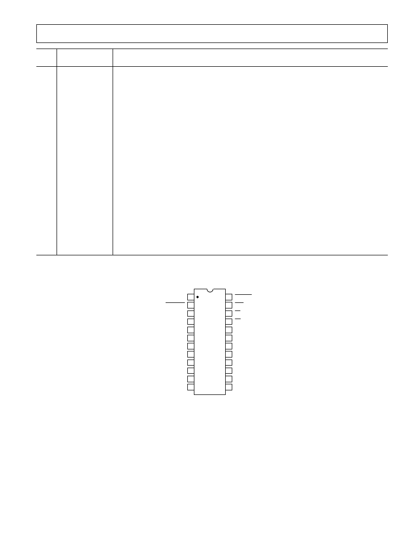
PIN CONFIGURATION
DIP and SOIC
V
DD
REF OUT/REF IN
AGND
MODE
DB0 (LSB)
DB1
DB2
V
IN2
V
IN1
DB11/LOW
DB3/
RFS
DB10/LOW
DB4/SCLK
DB9
DB5/SDATA
DB8
DGND
DB7
DB6
14
1
2
24
23
5
6
7
20
19
18
3
4
22
21
8
17
9
16
10
15
11
TOP VIEW
(Not to Scale)
12
13
AD7892
STANDBY
CONVST
EOC
CS
RD
相關PDF資料 |
PDF描述 |
|---|---|
| AD7892AN-1 | LC2MOS Single Supply, 12-Bit 600 kSPS ADC |
| AD7892AN-2 | LC2MOS Single Supply, 12-Bit 600 kSPS ADC |
| AD7892AN-3 | LC2MOS Single Supply, 12-Bit 600 kSPS ADC |
| AD7892AR-1 | LC2MOS Single Supply, 12-Bit 600 kSPS ADC |
| AD7892BN-1 | LC2MOS Single Supply, 12-Bit 600 kSPS ADC |
相關代理商/技術參數 |
參數描述 |
|---|---|
| AD7892SQ-1 | 功能描述:模數轉換器 - ADC Bipolar Input Parallel 12B 600kSPS RoHS:否 制造商:Analog Devices 通道數量: 結構: 轉換速率: 分辨率: 輸入類型: 信噪比: 接口類型: 工作電源電壓: 最大工作溫度: 安裝風格: 封裝 / 箱體: |
| AD7893ACHIPS-10 | 功能描述:12 Bit Analog to Digital Converter 1 Input 1 SAR Die 制造商:analog devices inc. 系列:- 包裝:托盤 - 晶粒 零件狀態:上次購買時間 位數:12 采樣率(每秒):117k 輸入數:1 輸入類型:單端 數據接口:SPI 配置:S/H-ADC 無線電 - S/H:ADC:1:1 A/D 轉換器數:1 架構:SAR 參考類型:外部 電壓 - 電源,模擬:5V 電壓 - 電源,數字:5V 特性:- 工作溫度:-40°C ~ 85°C 封裝/外殼:模具 供應商器件封裝:模具 標準包裝:1 |
| AD7893ACHIPS-2 | 功能描述:12 Bit Analog to Digital Converter 1 Input 1 SAR Die 制造商:analog devices inc. 系列:- 包裝:管件 零件狀態:上次購買時間 位數:12 采樣率(每秒):117k 輸入數:1 輸入類型:單端 數據接口:SPI 配置:S/H-ADC 無線電 - S/H:ADC:1:1 A/D 轉換器數:1 架構:SAR 參考類型:外部 電壓 - 電源,模擬:5V 電壓 - 電源,數字:5V 特性:- 工作溫度:-40°C ~ 85°C 封裝/外殼:模具 供應商器件封裝:模具 標準包裝:1 |
| AD7893ACHIPS-5 | 功能描述:12 Bit Analog to Digital Converter 1 Input 1 SAR Die 制造商:analog devices inc. 系列:- 包裝:托盤 - 晶粒 零件狀態:上次購買時間 位數:12 采樣率(每秒):117k 輸入數:1 輸入類型:單端 數據接口:SPI 配置:S/H-ADC 無線電 - S/H:ADC:1:1 A/D 轉換器數:1 架構:SAR 參考類型:外部 電壓 - 電源,模擬:5V 電壓 - 電源,數字:5V 特性:- 工作溫度:-40°C ~ 85°C 封裝/外殼:模具 供應商器件封裝:模具 標準包裝:1 |
| AD7893AN-10 | 功能描述:IC ADC 12BIT SRL T/H LP 8-DIP RoHS:否 類別:集成電路 (IC) >> 數據采集 - 模數轉換器 系列:- 標準包裝:1 系列:- 位數:14 采樣率(每秒):83k 數據接口:串行,并聯 轉換器數目:1 功率耗散(最大):95mW 電壓電源:雙 ± 工作溫度:0°C ~ 70°C 安裝類型:通孔 封裝/外殼:28-DIP(0.600",15.24mm) 供應商設備封裝:28-PDIP 包裝:管件 輸入數目和類型:1 個單端,雙極 |
發布緊急采購,3分鐘左右您將得到回復。