- 您現(xiàn)在的位置:買賣IC網(wǎng) > PDF目錄373924 > AD7891 (Analog Devices, Inc.) 14-Bit 50 kSPS ADC Ser. Out, 1.8V Operation 8-MSOP PDF資料下載
參數(shù)資料
| 型號(hào): | AD7891 |
| 廠商: | Analog Devices, Inc. |
| 英文描述: | 14-Bit 50 kSPS ADC Ser. Out, 1.8V Operation 8-MSOP |
| 中文描述: | LC2MOS 8通道,12位高速數(shù)據(jù)采集系統(tǒng) |
| 文件頁數(shù): | 11/20頁 |
| 文件大小: | 173K |
| 代理商: | AD7891 |
AD7891
–11–
REV. A
Serial Interface Mode
The serial interface mode is selected by tying the MODE input
to a logic low. In this case, five of the data/control inputs of the
parallel mode assume serial interface functions.
The serial interface on the AD7891 is a five-wire interface with
read and write capabilities, with data being read from the output
register via the DATA OUT line and data being written to the
control register via the DATA IN line. The part operates in a
slave or external clocking mode and requires an externally ap-
plied serial clock to the SCLK input to access data from the
data register or write data to the control register. There are
separate framing signals for the read (
RFS
) and write (
TFS
)
operations. The serial interface on the AD7891 is designed to
allow the part to be interfaced to systems that provide a serial
clock that is synchronized to the serial data, such as the 80C51,
87C51, 68HC11 and 68HC05 and most digital signal processors.
When using the AD7891 in serial mode, the data lines DB11–
DB10 should be tied to logic low, and the
CS
,
WR
and
RD
inputs should be tied to logic high. Pins DB4–DB0 can be tied
to either logic high or logic low, but must not be left floating as
this condition could cause the AD7891 to draw large amounts
of current.
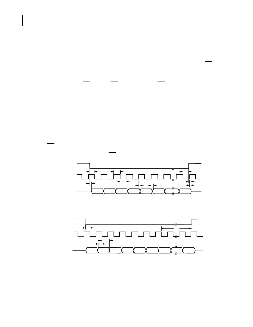
Read Operation
Figure 3 shows the timing diagram for reading from the AD7891
in serial mode.
RFS
goes low to access data from the AD7891.
The serial clock input does not have to be continuous. The serial
data can be accessed in a number of bytes. However,
RFS
must
remain low for the duration of the data transfer operation. Six-
teen bits of data are transmitted in serial mode with the data
FORMAT bit first, followed by the three address bits in the
control register, followed by the 12-bit conversion result starting
with the MSB. Serial data is clocked out of the device on the
rising edge of SCLK and is valid on the falling edge of SCLK.
At the end of the read operation, the DATA OUT line is three-
stated by a rising edge on either the SCLK or
RFS
inputs, which-
ever occurs first.
Write Operation
Figure 4 shows a write operation to the control register of the
AD7891. The
TFS
input goes low to indicate to the part that a
serial write is about to occur. The AD7891 Control Register
requires only six bits of data. These are loaded on the first six
clock cycles of the serial clock with data on all subsequent clock
cycles being ignored. Serial data to be written to the AD7891
must be valid on the falling edge of SCLK.
Simplifying the Serial Interface
To minimize the number of interconnect lines to the AD7891 in
serial mode, the user can connect the
RFS
and
TFS
lines of the
AD7891 together and read and write from the part simulta-
neously. In this case, new control register data line selecting the
input channel and providing a conversion start command should
be provided on the DATA IN line, while the part provides the
result from the conversion just completed on the DATA OUT
line.
DATA OUT (O)
SCLK (I)
RFS
(I)
t
18A
3-STATE
NOTE
I = INPUT
O = OUTPUT
FORMAT
A2
A1
A0
DB11
DB10
DB0
t
18
t
16
t
15
t
14
t
12
t
11
t
13
t
17
Figure 3. Serial Mode Read Operation
DATA IN (I)
SCLK (I)
TFS
(I)
NOTE
I = INPUT
FORMAT
A0
A1
A0
t
19
t
22
t
21
t
20
CONV
STBY
DONT
DONT
Figure 4. Serial Mode Write Operation
相關(guān)PDF資料 |
PDF描述 |
|---|---|
| AD7891AP-2 | LC2MOS 8-Channel, 12-Bit High Speed Data Acquisition System |
| AD7891AS-2 | LC2MOS 8-Channel, 12-Bit High Speed Data Acquisition System |
| AD7892AR-2 | LC2MOS Single Supply, 12-Bit 600 kSPS ADC |
| AD7892SQ-1 | LC2MOS Single Supply, 12-Bit 600 kSPS ADC |
| AD7892 | LC2MOS Single Supply, 12-Bit 600 kSPS ADC |
相關(guān)代理商/技術(shù)參數(shù) |
參數(shù)描述 |
|---|---|
| AD7891AP1 | 制造商:Analog Devices 功能描述: |
| AD7891AP-1 | 功能描述:IC DAS 12BIT 8CH 44-PLCC RoHS:否 類別:集成電路 (IC) >> 數(shù)據(jù)采集 - ADCs/DAC - 專用型 系列:- 產(chǎn)品培訓(xùn)模塊:Lead (SnPb) Finish for COTS Obsolescence Mitigation Program 標(biāo)準(zhǔn)包裝:50 系列:- 類型:數(shù)據(jù)采集系統(tǒng)(DAS) 分辨率(位):16 b 采樣率(每秒):21.94k 數(shù)據(jù)接口:MICROWIRE?,QSPI?,串行,SPI? 電壓電源:模擬和數(shù)字 電源電壓:1.8 V ~ 3.6 V 工作溫度:-40°C ~ 85°C 安裝類型:表面貼裝 封裝/外殼:40-WFQFN 裸露焊盤 供應(yīng)商設(shè)備封裝:40-TQFN-EP(6x6) 包裝:托盤 |
| AD7891AP-1REEL | 功能描述:IC DAS 12BIT 8CH 44-PLCC RoHS:否 類別:集成電路 (IC) >> 數(shù)據(jù)采集 - ADCs/DAC - 專用型 系列:- 產(chǎn)品培訓(xùn)模塊:Lead (SnPb) Finish for COTS Obsolescence Mitigation Program 標(biāo)準(zhǔn)包裝:50 系列:- 類型:數(shù)據(jù)采集系統(tǒng)(DAS) 分辨率(位):16 b 采樣率(每秒):21.94k 數(shù)據(jù)接口:MICROWIRE?,QSPI?,串行,SPI? 電壓電源:模擬和數(shù)字 電源電壓:1.8 V ~ 3.6 V 工作溫度:-40°C ~ 85°C 安裝類型:表面貼裝 封裝/外殼:40-WFQFN 裸露焊盤 供應(yīng)商設(shè)備封裝:40-TQFN-EP(6x6) 包裝:托盤 |
| AD7891AP2 | 制造商:Analog Devices 功能描述: |
| AD7891AP-2 | 功能描述:IC DAS 12BIT 8CH 44-PLCC RoHS:否 類別:集成電路 (IC) >> 數(shù)據(jù)采集 - ADCs/DAC - 專用型 系列:- 產(chǎn)品培訓(xùn)模塊:Lead (SnPb) Finish for COTS Obsolescence Mitigation Program 標(biāo)準(zhǔn)包裝:50 系列:- 類型:數(shù)據(jù)采集系統(tǒng)(DAS) 分辨率(位):16 b 采樣率(每秒):21.94k 數(shù)據(jù)接口:MICROWIRE?,QSPI?,串行,SPI? 電壓電源:模擬和數(shù)字 電源電壓:1.8 V ~ 3.6 V 工作溫度:-40°C ~ 85°C 安裝類型:表面貼裝 封裝/外殼:40-WFQFN 裸露焊盤 供應(yīng)商設(shè)備封裝:40-TQFN-EP(6x6) 包裝:托盤 |
發(fā)布緊急采購,3分鐘左右您將得到回復(fù)。