- 您現在的位置:買賣IC網 > PDF目錄373923 > AD7888 (Analog Devices, Inc.) +2.7 V to +5.25 V, Micropower, 8-Channel, 125 kSPS, 12-Bit ADC in 16-Lead TSSOP PDF資料下載
參數資料
| 型號: | AD7888 |
| 廠商: | Analog Devices, Inc. |
| 英文描述: | +2.7 V to +5.25 V, Micropower, 8-Channel, 125 kSPS, 12-Bit ADC in 16-Lead TSSOP |
| 中文描述: | 2.7 V至5.25 V,微功耗,8通道,125 kSPS的,12位ADC的16引腳TSSOP |
| 文件頁數: | 8/16頁 |
| 文件大小: | 164K |
| 代理商: | AD7888 |
REV. 0
AD7888
–8–
Figure 4 shows the typical power supply rejection ratio vs.
frequency for the part. The power supply rejection ratio is de-
fined as the ratio of the power in the ADC output at frequency f
to the power of a full-scale sine wave applied to the ADC of
frequency f
S
:
PSRR (dB) =
10 log
(Pf/Pfs)
Pf
= Power at frequency
f
in ADC output,
Pfs
= power at fre-
quency fs in ADC full scale input. Here a 100 mV peak-to-peak
sine wave is coupled onto the V
DD
supply. Both the +2.7 V and
+5.5 V supply performances are shown.
INPUT FREQUENCY – kHz
–93
2.65
64.15
P
12.85
33.65
V
DD
= +5.5V/+2.7V
100mV p-p SINE WAVE ON V
REF
IN
= 2.488V EXT REFERENCE
23.15
–91
–89
–87
–85
–83
–81
–79
–77
–75
43.85
54.35
Figure 4. PSRR vs. Frequency
CIRCUIT INFORMATION
The AD7888 is a fast, low power, 12-bit, single supply, 8-
channel A/D converter. The part can be operated from +3 V
(+2.7 V to +3.6 V) supply or from +5 V (+4.75 V to +5.25 V)
supply. When operated from either a +5 V supply or a +3 V
supply, the AD7888 is capable of throughput rates of 125 kSPS
when provided with a 2 MHz clock.
The AD7888 provides the user with an 8-channel multiplexer,
on-chip track/hold, A/D converter, reference and serial interface
housed in a tiny 16-lead TSSOP package, which offers the user
considerable space saving advantages over alternative solutions.
The serial clock input accesses data from the part and also
provides the clock source for the successive-approximation
A/D converter. The analog input range is 0 to V
REF
(where
the externally-applied V
REF
can be between +1.2 V and V
DD
).
The 8-channel multiplexer is controlled by the part’s Control
Register. This Control Register also allows the user to power-off
the internal reference and to determine the Modes of Operation.
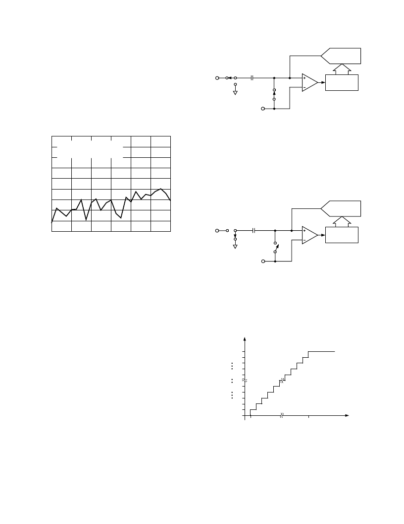
CONVERTER OPERATION
The AD7888 is a successive-approximation analog-to-digital
converter based around a charge redistribution DAC. Figures 5
and 6 show simplified schematics of the ADC. Figure 5 shows
the ADC during its acquisition phase. SW2 is closed and SW1 is
in Position A, the comparator is held in a balanced condition
and the sampling capacitor acquires the signal on AIN.
CHARGE
REDISTRIBUTION
DAC
(REF IN/REF OUT)/2
SAMPLING
CAPACITOR
COMPARATOR
CONTROL
LOGIC
ACQUISITION
PHASE
SW1
A
SW2
AGND
B
AIN
Figure 5. ADC Acquisition Phase
When the ADC starts a conversion, (see Figure 6), SW2 will
open and SW1 will move to Position B causing the comparator
to become unbalanced. The control logic and the charge redis-
tribution DAC are used to add and subtract fixed amounts of
charge from the sampling capacitor to bring the comparator
back into a balanced condition. When the comparator is rebal-
anced, the conversion is complete. The control logic generates
the ADC output code. Figure 7 shows the ADC transfer
function.
CONVERSION
PHASE
CHARGE
REDISTRIBUTION
DAC
(REF IN/REF OUT)/2
SAMPLING
CAPACITOR
COMPARATOR
CONTROL
LOGIC
SW1
A
SW2
AGND
B
VIN
Figure 6. ADC Conversion Phase
ADC TRANSFER FUNCTION
The output coding of the AD7888 is straight binary. The de-
signed code transitions occur at successive integer LSB values
(i.e., 1 LSB, 2 LSBs, etc.). The LSB size is = V
REF
/4096. The
ideal transfer characteristic for the AD7888 is shown in Figure 7
below.
0V
A
ANALOG INPUT
111...000
011...111
0.5LSB
+V
REF
– 1.5LSB
1LSB = V
REF
/4096
111...111
111...110
000...010
000...001
000...000
Figure 7. Transfer Characteristic
相關PDF資料 |
PDF描述 |
|---|---|
| AD7888AR | +2.7 V to +5.25 V, Micropower, 8-Channel, 125 kSPS, 12-Bit ADC in 16-Lead TSSOP |
| AD7888ARU | +2.7 V to +5.25 V, Micropower, 8-Channel, 125 kSPS, 12-Bit ADC in 16-Lead TSSOP |
| AD7888BR | +2.7 V to +5.25 V, Micropower, 8-Channel, 125 kSPS, 12-Bit ADC in 16-Lead TSSOP |
| AD7888BRU | +2.7 V to +5.25 V, Micropower, 8-Channel, 125 kSPS, 12-Bit ADC in 16-Lead TSSOP |
| AD7889 | 12-Bit 600 kSPS ADC(單電源600kSPS12位A/D轉換器) |
相關代理商/技術參數 |
參數描述 |
|---|---|
| AD7888AR | 制造商:Analog Devices 功能描述:ADC Single SAR 125ksps 12-bit Serial 16-Pin SOIC N 制造商:Analog Devices 功能描述:IC 12BIT ADC 8CH MICROPOWER 7888 |
| AD7888AR-REEL | 制造商:Analog Devices 功能描述:ADC Single SAR 125ksps 12-bit Serial 16-Pin SOIC N T/R |
| AD7888AR-REEL7 | 制造商:Analog Devices 功能描述:ADC Single SAR 125ksps 12-bit Serial 16-Pin SOIC N T/R |
| AD7888ARU | 功能描述:IC ADC 12BIT 8CH 125KSPS 16TSSOP RoHS:否 類別:集成電路 (IC) >> 數據采集 - 模數轉換器 系列:- 標準包裝:1,000 系列:- 位數:12 采樣率(每秒):300k 數據接口:并聯 轉換器數目:1 功率耗散(最大):75mW 電壓電源:單電源 工作溫度:0°C ~ 70°C 安裝類型:表面貼裝 封裝/外殼:24-SOIC(0.295",7.50mm 寬) 供應商設備封裝:24-SOIC 包裝:帶卷 (TR) 輸入數目和類型:1 個單端,單極;1 個單端,雙極 |
| AD7888ARU-REEL | 功能描述:IC ADC 12BIT 8CH SRL 16-TSSOP RoHS:否 類別:集成電路 (IC) >> 數據采集 - 模數轉換器 系列:- 標準包裝:1,000 系列:- 位數:16 采樣率(每秒):45k 數據接口:串行 轉換器數目:2 功率耗散(最大):315mW 電壓電源:模擬和數字 工作溫度:0°C ~ 70°C 安裝類型:表面貼裝 封裝/外殼:28-SOIC(0.295",7.50mm 寬) 供應商設備封裝:28-SOIC W 包裝:帶卷 (TR) 輸入數目和類型:2 個單端,單極 |
發布緊急采購,3分鐘左右您將得到回復。