- 您現在的位置:買賣IC網 > PDF目錄373923 > AD7886JP (ANALOG DEVICES INC) LC2MOS 12-Bit, 750 kHz/1 MHz, Sampling ADC PDF資料下載
參數資料
| 型號: | AD7886JP |
| 廠商: | ANALOG DEVICES INC |
| 元件分類: | ADC |
| 英文描述: | LC2MOS 12-Bit, 750 kHz/1 MHz, Sampling ADC |
| 中文描述: | 1-CH 12-BIT FLASH METHOD ADC, PARALLEL ACCESS, PQCC28 |
| 封裝: | PLASTIC, LCC-28 |
| 文件頁數: | 5/16頁 |
| 文件大小: | 400K |
| 代理商: | AD7886JP |
AD7886
–5–
REV. B
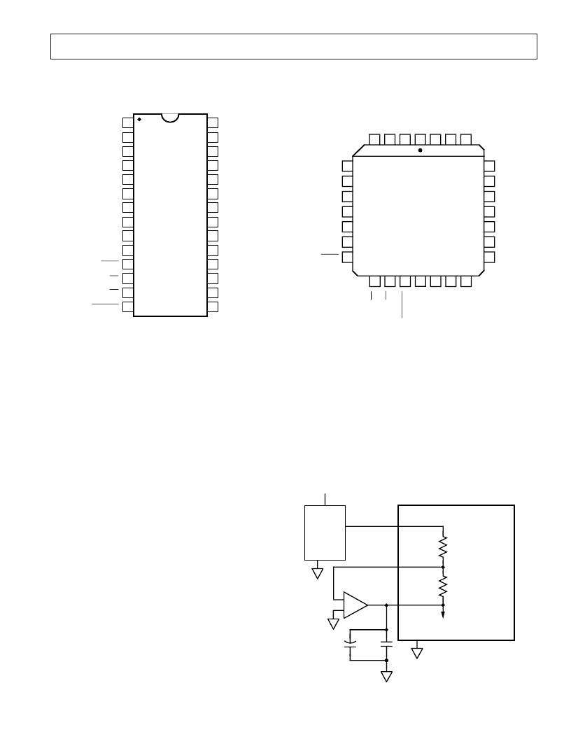
PIN CONFIGURATIONS
DIP
1
2
3
4
5
6
7
8
9
10
11
12
13
14
28
27
26
25
24
23
22
21
20
19
18
17
16
15
TOP VIEW
(Not to Scale)
AD7886
DB7
DB6
DB5
DB4
DGND
DB3
DB2
DB1
DB0
V
DD
DB8
DB9
DB10
DB11
V
SS
AGND
V
REF
SUM
+5REF
V
DD
VIN2
VIN1
AGND
V
SS
CS
RD
CONVST
BUSY
TERMINOLOGY
Unipolar Offset Error
The ideal first code transition should occur when the analog
input is 1 LSB above AGND. The deviation of the actual transi-
tion from that point is termed the offset error.
Bipolar Zero Error
The ideal midscale transition (i.e., 0111 1111 1111 to 1000
0000 0000) for the +5 V range should occur when the analog
input is at zero volts. Bipolar zero error is the deviation of the
actual transition from that point.
Gain Error
In the unipolar mode, gain error is measured with respect to the
first and last code transition points. The ideal difference be-
tween these points is FS–2 LSBs. For bipolar applications, the
gain error is measured from the midscale transition to both the
first and last code transitions. The ideal difference in this case is
FS/2–1 LSB. The gain error is defined as the deviation between
the ideal difference, given above, and the measured difference.
For the bipolar case, there are two gain errors; the figure in the
specification page represents the worst case. Ideal FS depends
on the +5REF input; for the 0 V to 5 V input, ideal FS = +5REF
and for the 0 V to 10 V and +5 V ranges, ideal FS = 2
×
+ 5REF.
CONVERTER DETAILS
The AD7886 is a triple-pass flash ADC that uses 15 compara-
tors in a 4-bit flash technique to perform the 12-bit conversion
procedure. Each of the 4096 quantization levels is realized inter-
nally with a precision resistor DAC.
The fifteen comparators first compare the analog input voltage
to the V
REF
/16 voltages of the resistor array. This determines the
four most significant bits and selects 1 out of 16 voltage seg-
ments. The comparators are then switched to 15 subvoltages on
that segment to determine the next four bits and select 1 out of
256 voltage segments. A further switching of the comparators to
another 15 subvoltages produces the complete 12-bit conversion
result. The 12 bits of data are then stored internally in a three-
state output latch.
REFERENCE INPUT
The AD7886 operates from a 3.5 V reference, which must be
provided at the V
REF
input. Two on-chip resistors for use with
an external amplifier can be used for deriving 3.5 V from stan-
dard 5 V references. Figure 2 shows an example with the AD586
which a is a high performance voltage reference exhibiting
excellent stability performance, 5 ppm/
°
C max. The external
amplifier serves a second function of force/sensing the V
REF
input. Force/sensing minimizes error contributions from
AD7886*
SUM
+5REF
TO DAC
+
–
AD586
V
OUT
+V
IN
GND
AGND
+V
+5V
R1
9k
R2
6.3k
C1
10
μ
F
C2
0.1
μ
F
AD707
V
REF
–3.5V
*ADDITIONAL PINS OMITTED FOR CLARITY
Figure 2. Typical Reference Circuitry
PLCC
A
V
V
D
D
D
DB11
D
D
D
D
AGND
SUM
+5REF
DB2
DB1
DB0
DGND
DB3
V
SS
V
REF
V
DD
C
R
C
V
S
V
DD
BUSY
AD7886
TOP VIEW
(Not to Scale)
5
6
7
8
9
10
11
28
27
26
1
2
3
4
25
24
23
22
21
20
19
12
13
14
15
16
17
18
相關PDF資料 |
PDF描述 |
|---|---|
| AD7886 | LC2MOS 12-Bit, 750 kHz/1 MHz, Sampling ADC |
| AD7886BD | LC2MOS 12-Bit, 750 kHz/1 MHz, Sampling ADC |
| AD7886KD | LC2MOS 12-Bit, 750 kHz/1 MHz, Sampling ADC |
| AD7886KP | LC2MOS 12-Bit, 750 kHz/1 MHz, Sampling ADC |
| AD7886TD | LC2MOS 12-Bit, 750 kHz/1 MHz, Sampling ADC |
相關代理商/技術參數 |
參數描述 |
|---|---|
| AD7886JP-REEL | 功能描述:IC ADC 12BIT SAMPLING HS 28-PLCC RoHS:否 類別:集成電路 (IC) >> 數據采集 - 模數轉換器 系列:- 標準包裝:1 系列:- 位數:14 采樣率(每秒):83k 數據接口:串行,并聯 轉換器數目:1 功率耗散(最大):95mW 電壓電源:雙 ± 工作溫度:0°C ~ 70°C 安裝類型:通孔 封裝/外殼:28-DIP(0.600",15.24mm) 供應商設備封裝:28-PDIP 包裝:管件 輸入數目和類型:1 個單端,雙極 |
| AD7886KP-REEL | 制造商:Analog Devices 功能描述: |
| AD7887AR | 功能描述:IC ADC 12BIT 2CH SRL 8-SOIC RoHS:否 類別:集成電路 (IC) >> 數據采集 - 模數轉換器 系列:- 標準包裝:1,000 系列:- 位數:16 采樣率(每秒):45k 數據接口:串行 轉換器數目:2 功率耗散(最大):315mW 電壓電源:模擬和數字 工作溫度:0°C ~ 70°C 安裝類型:表面貼裝 封裝/外殼:28-SOIC(0.295",7.50mm 寬) 供應商設備封裝:28-SOIC W 包裝:帶卷 (TR) 輸入數目和類型:2 個單端,單極 |
| AD7887ARM | 功能描述:IC ADC 12BIT 2CH SRL 8-MSOP RoHS:否 類別:集成電路 (IC) >> 數據采集 - 模數轉換器 系列:- 標準包裝:1,000 系列:- 位數:16 采樣率(每秒):45k 數據接口:串行 轉換器數目:2 功率耗散(最大):315mW 電壓電源:模擬和數字 工作溫度:0°C ~ 70°C 安裝類型:表面貼裝 封裝/外殼:28-SOIC(0.295",7.50mm 寬) 供應商設備封裝:28-SOIC W 包裝:帶卷 (TR) 輸入數目和類型:2 個單端,單極 |
| AD7887ARM-REEL | 制造商:Analog Devices 功能描述:ADC Single SAR 125ksps 12-bit Serial 8-Pin MSOP T/R |
發布緊急采購,3分鐘左右您將得到回復。