- 您現在的位置:買賣IC網 > PDF目錄373920 > AD7854L (Analog Devices, Inc.) 12-Bit Sampling ADC(單電源,200kSPS 12位采樣A/D轉換器) PDF資料下載
參數資料
| 型號: | AD7854L |
| 廠商: | Analog Devices, Inc. |
| 英文描述: | 12-Bit Sampling ADC(單電源,200kSPS 12位采樣A/D轉換器) |
| 中文描述: | 12位采樣ADC(單電源,速度高達200ksps的12位采樣的A / D轉換器) |
| 文件頁數: | 3/28頁 |
| 文件大小: | 268K |
| 代理商: | AD7854L |
第1頁第2頁當前第3頁第4頁第5頁第6頁第7頁第8頁第9頁第10頁第11頁第12頁第13頁第14頁第15頁第16頁第17頁第18頁第19頁第20頁第21頁第22頁第23頁第24頁第25頁第26頁第27頁第28頁
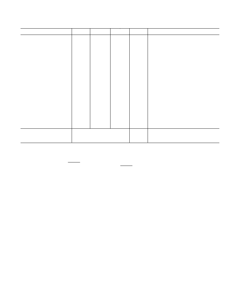
Parameter
A Version
1
B Version
1
S Version
1
Units
T est Conditions/Comments
POWER REQUIREMENT S
AV
DD,
DV
DD
I
DD
Normal Mode
5
+3.0/+5.5
+3.0/+5.5
+3.0/+5.5
V min/max
5.5 (1.8)
5.5 (1.8)
6 (1.8)
mA max
AV
DD
= DV
DD
= 4.5 V to 5.5 V. T ypically 4.5 mA
(1.5 mA);
AV
DD
= DV
DD
= 3.0 V to 3.6 V. T ypically 4.0 mA
(1.5 mA).
5.5 (1.8)
5.5 (1.8)
6 (1.8)
mA max
Sleep Mode
6
With External Clock On
10
10
10
μ
A typ
Full power-down. Power management bits in control
register set as PMGT 1 = 1, PMGT 0 = 0.
Partial power-down. Power management bits in
control register set as PMGT 1 = 1, PMGT 0 = 1.
T ypically 1
μ
A. Full power-down. Power management
bits in control register set as PMGT 1 = 1,
PMGT 0 = 0.
Partial power-down. Power management bits in
control register set as PMGT 1 = 1, PMGT 0 = 1.
V
DD
= 5.5 V: T ypically 25 mW (8)
V
DD
= 3.6 V: T ypically 15 mW (5.4)
400
400
400
μ
A typ
With External Clock Off
5
5
5
μ
A max
200
200
200
μ
A typ
Normal Mode Power Dissipation
30 (10)
20 (6.5)
30 (10)
20 (6.5)
30 (10)
20 (6.5)
mW max
mW max
Sleep Mode Power Dissipation
With External Clock On
55
36
27.5
18
55
36
27.5
18
55
36
27.5
18
μ
W typ
μ
W typ
μ
W max
μ
W max
V
DD
= 5.5 V
V
DD
= 3.6 V
V
DD
= 5.5 V: T ypically 5.5
μ
W
V
DD
= 3.6 V: T ypically 3.6
μ
W
With External Clock Off
SYST EM CALIBRAT ION
Offset Calibration Span
7
Gain Calibration Span
7
+0.05
×
V
REF
/–0.05
×
V
REF
+0.025
×
V
REF
/–0.025
×
V
REF
V max/min
V max/min
Allowable Offset Voltage Span for Calibration
Allowable Full-Scale Voltage Span for Calibration
NOT ES
1
T emperature ranges as follows: A, B Versions, –40
°
C to +85
°
C; S Version, –55
°
C to +125
°
C.
2
Specifications apply after calibration.
3
Not production tested. Guaranteed by characterization at initial product release.
4
Sample tested @ +25
°
C to ensure compliance.
5
All digital inputs @ DGND except for
CONVST
@ DV
. No load on the digital outputs. Analog inputs @ AGND.
6
CLK IN @ DGND when external clock off. All digital inputs @ DGND except for
CONVST
@ DV
. No load on the digital outputs. Analog inputs @ AGND.
7
T he offset and gain calibration spans are defined as the range of offset and gain errors that the AD7854/AD7854L can calibrate. Note also that these are voltage spans
and are not absolute voltages (i.e., the allowable system offset voltage presented at AIN(+) for the system offset error to be adjusted out will be AIN(–)
±
0.05
×
V
REF
,
and the allowable system full-scale voltage applied between AIN(+) and AIN(–) for the system full-scale voltage error to be adjusted out will be V
REF
±
0.025
×
V
REF
(unipolar mode) and V
REF
/2
±
0.025
×
V
REF
(bipolar mode)). T his is explained in more detail in the calibration section of the data sheet.
Specifications subject to change without notice.
REV. 0
–3–
AD7854/AD7854L
相關PDF資料 |
PDF描述 |
|---|---|
| AD7854 | 12-Bit Sampling ADC(單電源,200kSPS 12位采樣A/D轉換器) |
| AD7858LARS | 3 V to 5 V Single Supply, 200 kSPS 8-Channel, 12-Bit Sampling ADC |
| AD7858BN | 3 V to 5 V Single Supply, 200 kSPS 8-Channel, 12-Bit Sampling ADC |
| AD7858BR | 3 V to 5 V Single Supply, 200 kSPS 8-Channel, 12-Bit Sampling ADC |
| AD7858AN | 3 V to 5 V Single Supply, 200 kSPS 8-Channel, 12-Bit Sampling ADC |
相關代理商/技術參數 |
參數描述 |
|---|---|
| AD7854LAQ | 制造商:Rochester Electronics LLC 功能描述:12 BIT SINGLE CHANNEL PARALLEL ADC I.C. - Bulk |
| AD7854LAR | 制造商:Analog Devices 功能描述:ADC Single SAR 100ksps 12-bit Parallel 28-Pin SOIC W 制造商:Rochester Electronics LLC 功能描述:12-BIT SINGLE CHANNEL PARALLEL ADC I.C. - Bulk |
| AD7854LAR-REEL | 制造商:Analog Devices 功能描述:ADC Single SAR 100ksps 12-bit Parallel 28-Pin SOIC W T/R 制造商:Analog Devices 功能描述:ADC SGL SAR 100KSPS 12-BIT PARALLEL 28SOIC W - Tape and Reel |
| AD7854LARS | 功能描述:IC ADC 12BIT PARALLEL LP 28-SSOP RoHS:否 類別:集成電路 (IC) >> 數據采集 - 模數轉換器 系列:- 產品培訓模塊:Lead (SnPb) Finish for COTS Obsolescence Mitigation Program 標準包裝:2,500 系列:- 位數:12 采樣率(每秒):3M 數據接口:- 轉換器數目:- 功率耗散(最大):- 電壓電源:- 工作溫度:- 安裝類型:表面貼裝 封裝/外殼:SOT-23-6 供應商設備封裝:SOT-23-6 包裝:帶卷 (TR) 輸入數目和類型:- |
發布緊急采購,3分鐘左右您將得到回復。