- 您現在的位置:買賣IC網 > PDF目錄373918 > AD7828 (Analog Devices, Inc.) 2.7V-5.25V Digital, 5V Analog, 12 Bit, 4MSPS, Parallel ADC with Ref 48-TQFP -40 to 85 PDF資料下載
參數資料
| 型號: | AD7828 |
| 廠商: | Analog Devices, Inc. |
| 英文描述: | 2.7V-5.25V Digital, 5V Analog, 12 Bit, 4MSPS, Parallel ADC with Ref 48-TQFP -40 to 85 |
| 中文描述: | LC2MOS高速4 - |
| 文件頁數: | 9/16頁 |
| 文件大小: | 270K |
| 代理商: | AD7828 |
AD7824/AD7828
REV. F
–9–
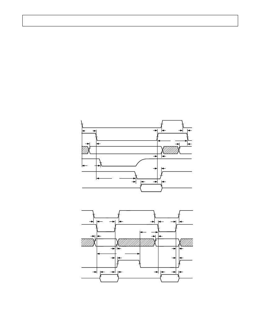
MODE 0
Figure 14 shows the timing diagram for Mode 0 operation. This
mode can only be used for microprocessors that have a WAIT
state facility, whereby a READ instruction cycle can be extended
to accommodate slow memory devices. A READ operation brings
CS
and
RD
low, which starts a conversion. The analog multiplexer
address inputs must remain valid while
CS
and
RD
are low. The
data bus (DB7–DB0) remains in the three-state condition until
conversion is complete. There are two converter status outputs on
the AD7824/AD7828, interrupt (
INT
) and ready (RDY), which
can be used to drive the microprocessor READY/WAIT input.
The RDY is an open-drain output (no internal pull-up device) that
goes low on the falling edge of
CS
and goes high impedance at the
end of conversion when the 8-bit conversion result appears on the
data outputs. If the RDY status is not required, the external
pull-up resistor can be omitted and the RDY output tied to GND.
The
INT
goes low when conversion is complete and returns high
on the rising edge of
CS
or
RD
.
MODE 1
Mode 1 operation is designed for applications where the micropro-
cessor is not forced into a WAIT state. A READ operation takes
CS
and
RD
low, which triggers a conversion (see Figure 15). The
multiplexer address inputs are latched on the rising edge of
RD
.
Data from the previous conversion is read from the three-state
data outputs (DB7–DB0). This data may be disregarded if not
required. Note that the RDY output (open drain output) does
not provide any status information in this mode and must be
connected to GND. At the end of conversion,
INT
goes low. A
second READ operation is required to access the new conversion
result. This READ operation latches a new address into the multi-
plexer inputs and starts another conversion.
INT
returns high at the
end of the second READ operation, when
CS
or
RD
returns high.
A delay of 2.5
μ
s must be allowed between READ operations.
CS
RD
ANALOG
CHANNEL
ADDRESS
RDY
INT
DATA
t
CSS
t
AS
t
RDY
t
CRD
t
ACC2
t
DH
t
INTH
t
AH
t
AS
t
P
t
CSS
t
CSH
ADDRESS
VALID
ADDRESS
VALID
DATA
VALID
HIGH IMPEDANCE
Figure 14. Mode 0 Timing Diagram
CS
RD
ANALOG
CHANNEL
ADDRESS
INT
DATA
t
CSS
t
AS
ADDRESS
VALID
OLD
VALID
ADDRESS
VALID
NEW
VALID
t
CSH
t
AH
t
RD
t
CRD
t
INTH
t
ACC1
t
DH
t
ACC1
t
DH
t
INTH
t
AH
t
AS
t
P
t
CSS
t
RD
t
CSH
Figure 15. Mode 1 Timing Diagram
相關PDF資料 |
PDF描述 |
|---|---|
| AD7828BQ | LC2MOS High Speed 4- & 8-Channel 8-Bit ADCs |
| AD7828BR | 2.7V-5.25V Digital, 5V Analog, 12 Bit, 4MSPS, Parallel ADC with Ref 48-TQFP -40 to 85 |
| AD7828BRS | LC2MOS High Speed 4- & 8-Channel 8-Bit ADCs |
| AD7828LP | LC2MOS High Speed 4- & 8-Channel 8-Bit ADCs |
| AD7824CQ | TRANS ARRAY PNP/PNP SSS MINI-6P |
相關代理商/技術參數 |
參數描述 |
|---|---|
| AD7828BCHIPS | 制造商:未知廠家 制造商全稱:未知廠家 功能描述:Single-Ended Data Acquisition System |
| AD7828BQ | 功能描述:IC ADC 8BIT 8CH HS 28-CDIP RoHS:否 類別:集成電路 (IC) >> 數據采集 - 模數轉換器 系列:- 標準包裝:1 系列:- 位數:14 采樣率(每秒):83k 數據接口:串行,并聯 轉換器數目:1 功率耗散(最大):95mW 電壓電源:雙 ± 工作溫度:0°C ~ 70°C 安裝類型:通孔 封裝/外殼:28-DIP(0.600",15.24mm) 供應商設備封裝:28-PDIP 包裝:管件 輸入數目和類型:1 個單端,雙極 |
| AD7828BR | 功能描述:IC ADC 8BIT 8CH HS 28-SOIC RoHS:否 類別:集成電路 (IC) >> 數據采集 - 模數轉換器 系列:- 標準包裝:1,000 系列:- 位數:12 采樣率(每秒):300k 數據接口:并聯 轉換器數目:1 功率耗散(最大):75mW 電壓電源:單電源 工作溫度:0°C ~ 70°C 安裝類型:表面貼裝 封裝/外殼:24-SOIC(0.295",7.50mm 寬) 供應商設備封裝:24-SOIC 包裝:帶卷 (TR) 輸入數目和類型:1 個單端,單極;1 個單端,雙極 |
| AD7828BR-REEL | 制造商:Analog Devices 功能描述:ADC Single Semiflash 50ksps 8-bit Parallel 28-Pin SOIC W T/R 制造商:Analog Devices 功能描述:CONVERTER I.C. - Tape and Reel |
| AD7828BRS | 制造商:AD 制造商全稱:Analog Devices 功能描述:LC2MOS High Speed 4- & 8-Channel 8-Bit ADCs |
發布緊急采購,3分鐘左右您將得到回復。